From Lab to Museum: Resonant Mie Voids Create Nanoscale Artworks with Exceptional Optical Properties
Advancements in nanotechnology and photonics are transforming various industries, offering exciting possibilities for metadevices and nanoscale optical sensors. However, manipulating light on the nanoscale has been challenging due to intrinsic losses in metals and dielectrics. A group of researchers around Mario Hentschel and Harald Giessen from the University of Stuttgart have addressed this issue with a groundbreaking strategy: resonant sub-wavelength localized confinement of light in air. This innovative approach not only enhances performance, but also opens doors for nanoscale color printing and art replication.
Unlocking the Power of Resonant Mie Voids
Dielectric systems have gained attention for their lower loss and flexibility. By creating voids within high-index dielectric materials, the researchers discovered localized resonant modes with exceptional optical properties. They used their Raith ionLINE (now VELION) FIB system to mill cylindrical holes into bulk silicon wafers with single-charged gold ions. This gave them the possibility to utilize the intrinsic depth variation capability in order to create voids with varying diameter and depth––a crucial factor for their resonant behavior.
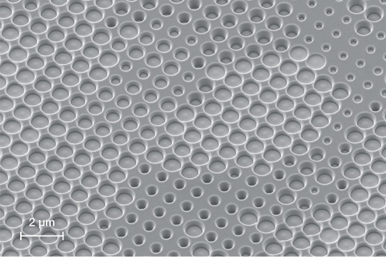
Unlike traditional systems, these resonant Mie voids confine light within air voids, eliminating loss and dispersion issues. This breakthrough enables effective manipulation of UV radiation, pushing the operation of high-index metasurfaces into the visible and UV spectral range.
Nanoscale Color Printing: A Fusion of Art and Science
Resonant Mie voids display brilliant and naturalistic colors in their scattering response, making them ideal for nanoscale color printing. A “color catalog” using arrays of voids with varying diameters and depths was created, reproducing a wide range of colors across the visible spectrum. To demonstrate the potential, Mario Hentschel et al. chose the painting “Improvisation No. 9″ by Wassily Kandinsky and printed a section of it using arrays of Mie voids. The resulting nanoscale color print can currently be viewed in the Staatsgalerie Stuttgart, where it will be displayed under a microscope next to the original for about five months. The “Nano-Kandinsky” is remarkably detailed, showcasing vivid and naturalistic colors against the silicon background. With a resolution of 36,000 dots per inch (dpi), these miniature color prints are astonishingly detailed, capturing the essence of the original artwork at a nanoscale level. Moreover, the use of silicon as the substrate ensures the stability of these prints over extended periods due to the material’s inertness and hardness. It showcases how this technique also offers an exciting new frontier for art reproduction and preservation.
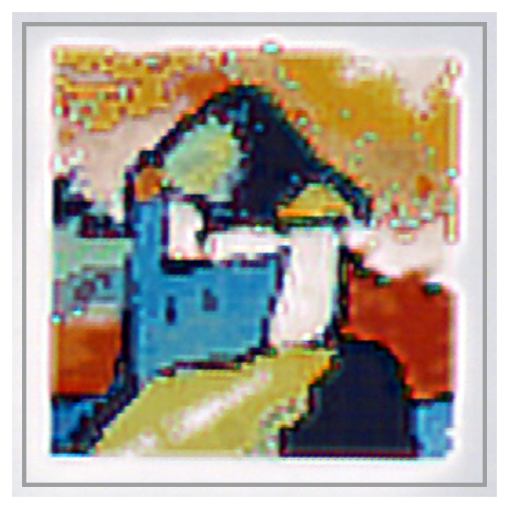
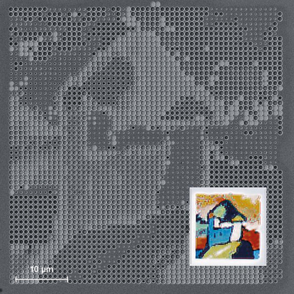
“Nano-Kansinsky” printed with arrays of Mie voids
Versatile Applications of Resonant Mie Voids
The practical applications of resonant Mie voids are vast and promising. The researchers demonstrated that these voids enable resonant light confinement down to the UV spectral range at 265 nm (4.68 eV) and utilized the bright, intense, and naturalistic colors produced by the voids for nanoscale color printing. This opens up new opportunities in various industries where precise and vibrant color reproduction is crucial.
Additionally, the combination of resonant dielectric Mie voids with dielectric nanoparticles provides an expanded parameter space for designing metasurfaces and other micro- and nanoscale optical elements. This extension allows for novel antenna and structure designs, leveraging the full access to the modal field inside the void, as well as the freedom to choose high-index materials for innovative sensing and active manipulation strategies.
Unlimited possibilities
The fabrication of resonant Mie voids as cylindrical holes of varying diameters and depths represents a significant milestone in dielectric nanophotonics. By confining light in air voids, this strategy overcomes the limitations of traditional high-index dielectric materials, enabling resonant light confinement in the visible and UV spectral range. From nanoscale color printing to advanced sensing and manipulation techniques, the applications are vast and promising.
Crucial for the creation and functionality of the resonant Mie voids was the precise fabrication of the varying holes. This was made possible by the top-down FIB geometry of VELION, a FIB system with a laser-interferometer stage and high stability which ensured the necessary high accuracy. As a further essential function, the system also offered the possibility of using gold ions for milling the structure. By making use of the multi-ion species ion source with gold and silicon ions, the researchers were able to choose the ion beam that was best suited to their application. Find out more about the multi-ion-species FIB-SEM VELION.
P.S.: Mario Hentschel’s picture “Nanoscale Colour printing with visible resonant Mie voids” also won second place in this year’s Micrograph Award. Check out all the winners here.