Laser stage technology for nm-precise sample positioning control
The field of nanofabrication in general, and specifically that of electron beam lithography, are concerned with getting a (CAD/GDSII) design down onto a sample for device manufacturing.
This can happen by means of a direct milling process, perhaps using FIB or resist chemical modification for electron beam lithography, the latter with a subsequent development and pattern transfer process. The broad scope of the application bandwidth is matched by the significant variations in size of the designs/devices – typically ranging from a few (tens of) microns to several mm and even up to the cm regime, and often repeating the device pattern across an entire wafer.
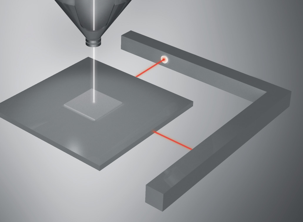
Charged particle beams such as electron or ion beams can be scanned/deflected over tool-specific areas only. Depending on the desired resolution and pattern placement accuracy, these write fields can reach a maximum of ~1 mm, thus limiting the maximum area that can be patterned in one go. This means designs larger than a single write field cannot be patterned without moving the sample stage underneath. Here, the importance of a high-precision laser interferometer stage comes into play.
By implementing and exploiting a classical Michelson interferometer (see image below) in X and Y direction to control positioning of the sample stage in a nanofabrication system, the positioning accuracy of the sample stage can be adjusted in the nm regime. A Michelson interferometer consists at minimum of mirrors M1 & M2 and a beam splitter M. In the figure below, a source S emits light that hits the beam splitter surface M at point C. As M is partially reflective, part of the light is transmitted through to point B while some is reflected in the direction of A. Both beams recombine at point C’ to produce an interference pattern incident on the detector at point E.
This interference pattern typically consists of fringes or lines of different intensity whose distances correlate to the wavelength of the laserlight. However, their intensity profiles can be analyzed, evaluated, and extrapolated by the detector electronics such that the resolution can be brought down to currently 1/4096 lamda, with lambda being the laser wavelength. For a standard HeNe laser this corresponds to a best measurement resolution of approx. 0.15 nm. A change in the position of mirrors M1 and M2 results in a change of the position of the fringes (or lines) in the interference pattern, which is measured as an intensity change by the detector electronics and then correlated to the change in the physical stage XY coordinate system.
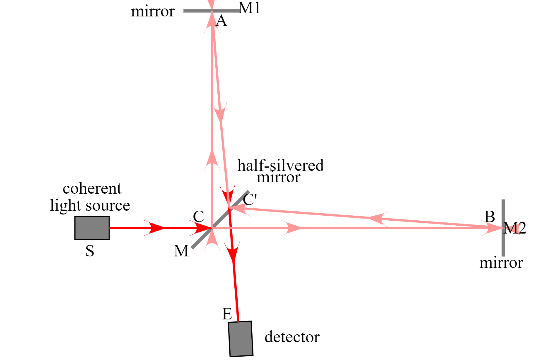
Path of light in Michelson interferometer - Krishnavedala (https://commons.wikimedia.org/wiki/File:Michelson_interferometer_with_labels.svg), „Michelson interferometer with labels“, https://creativecommons.org/licenses/by-sa/4.0/legalcode
Precise stitching for large-area devices
The highest positioning resolutions provided by this type of laser interferometer controlled stages are essential to fine-position the sample stage under the charged particle beam of a nanofabrication system such that individual write fields can be stitched together with nm precision.
Without laser interferometer control, the alternative requires reliance on the much worse positioning resolutions of optical encoders, which finally leads to stage positioning accuracies in the µm regime only (as is the case for regular SEMs or FIB-SEMs). When the stage is moved to the next adjacent write field position, this positioning inaccuracy would leave large unintentional gaps or overlaps between the write fields. Imagine a conducting line extending over a distance larger than the maximum field size, which could end in a voltage interruption that would most likely impair the device functionality or even totally destroy it.
True und unique closed-loop positioning control for Raith laser stages
The majority of Raith laser interferometer stages as integral parts of the nanofabrication systems come with true closed-loop feedback positioning control. This is realized by a combination of DC motors for rough positioning, working in parallel with Raith’s unique additional piezo blocks for fine positioning. The laser interferometer signal is monitored with high frequency and serves as direct closed-loop positioning feedback both to the DC motors and the piezo blocks of the motorized laser stage.
Raith laser stages designed following this concept are also capable of “continuous writing” modes. A specific operation mode allows both the ion or electron beam of the nanofabrication system and the laser stage to be moved synchronously using Raith’s unique proprietary fixed-beam moving stage (FBMS) and modulated-beam moving stage (MBMS) technology in its traxx and periodixx product options. With the help of these special operation modes, long elongated structures such as mm- and even cm-length waveguides and high-resolution gratings can be manufactured without stitching borders at all.
Find out more about traxx and periodixx here.
Highest write field size flexibility with no need for elaborate calibrations
Applying this concept, the stage can be positioned directly with nm accuracy following a true closed feedback loop principle. As a result, users can work directly and flexibly with write fields of any size. There is no need for specific calibration procedures, including beam positioning corrections, which are required for compensating rough stage positioning errors if operated by DC motors only.