References
All over the world, Raith systems are installed at universities, academic institutions, high technology companies, R&D centres, nano centres and governmental institutions. Leading-edge research and high-end technology are enabled with Raith systems every day.
Watch and read what some of our customers say about us:
Irfan Siddiqi about the EBPG at University of California, Berkeley
Stanley Lin and Richard Tiberio about the VOYAGER at Stanford University
Maribel Montero about the EBPG at University of California, San Diego
Dr. Matthias Hagner and Emilia Schütz talk about the PICOMASTER at the University of Konstanz, Germany.
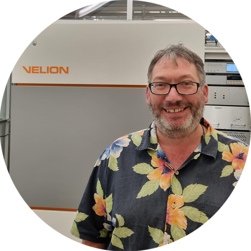
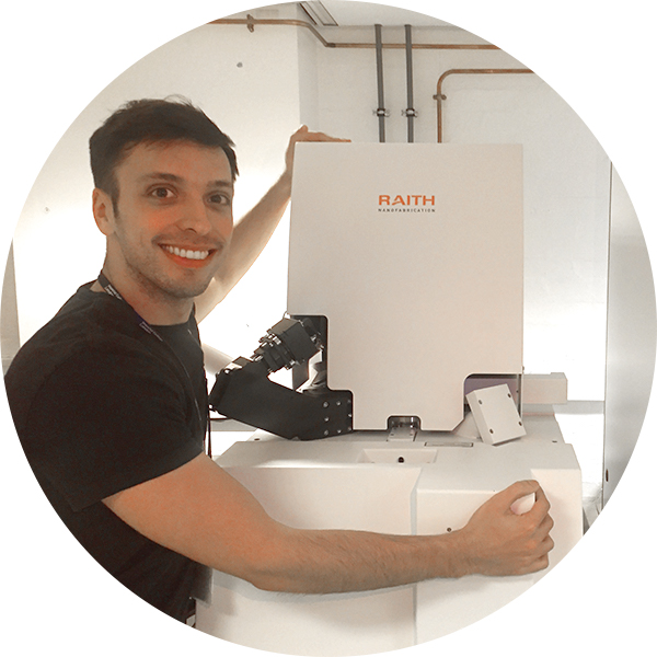
VELION at UC Santa Barbara
"We are extremely pleased with the versatility of the VELION tool installed in our multiuser facility at UCSB. Initially we worked with the more standard Au and Si ion beams but have recently enjoyed the enhanced resolution when patterning with Li ion in the GaBiLi source. My own personal research area of nanomagnetism for data storage applications has benefited from the capabilities of the VELION as we move from conventional 2D lithography to directly patterning quasi 3D materials."
Dr. Dan Read, University of California, Santa Barbara
ionLINE Plus and eLINE Plus at the University of Stuttgart
“Raith tools provide breakthrough technology at a very high level of reliability and reproducibility. This makes them real “paper machines” for our group. In the last year alone we published more than ten papers which would never have been possible without these systems.”
Prof. Dr. Harald Gießen, University of Stuttgart

VOYAGER at Stanford University
"The VOYAGER’s unique capabilities including traxx, periodixx, intrinsic circles, 10 kV and 50 kV modes complement our existing nanofabrication offerings covering a broad base of research needs. Moreover, Raith’s team of engineers are a great resource. Their remote access capability allows them to fix most issues effectively, increasing tool up-time."
Stanley Lin, Stanford University
VELION at the WWU Münster
"With its sophisticated FIB technology including non-Ga capabilities, highest-fidelity sample stage and dedicated patterning engine, VELION is the perfect addition to our set of instruments, and enables us to follow a dedicated strategy for extending R&D nanofabrication expertise and equipment.”
Prof. Dr. Wolfram Pernice, WWU Münster

EBPG at the Karlsruhe Institute of Technology
"The EBPG combines three functions essential in research: high precision, high flexibility and extreme reliability. The platform is easy to operate and can be used to produce reproducible nanostructures for optical applications. Overall, we are extremely satisfied with the EBPG and with Raith’s customer service.”
Dr. Lothar Hahn, KIT
eLINE Plus at the Max-Planck-Institute for Solid State Research, Stuttgart
"The Raith eLINE Plus is our standard tool for advanced nanofabrication. Its superior performance in terms of stability, reliability, and scalability lays the foundation for our scientific research, where the precise arrangement of plasmonic nanostructures over micrometer and centimeter sizes is key. In particular, its versatility is unequaled. It has enabled us to set and pursue novel research directions with completely different nanofabrication demands."
Prof. Dr. Na Liu, University of Stuttgart, Max-Planck-Institute for Solid State Research, Stuttgart

PIONEER at Queen's University
"The flexibility of the PIONEER was the deciding factor for us. While it is limited to 30 kV EHT and 50 mm wafers (and smaller chips), it is ideally suited for our R&D environment. Users appreciate the full control over parameters like acceleration voltage, working distance, etc., and with 7 different aperture sizes, they can access a wide range of beam current."
Graham Gibson, Queen's University
VOYAGER at the Virginia Commonwealth University
"The new Raith VOYAGER […] is a true game-changer. With the traxx and periodixx features and radically improved stage control, we are now able to seamlessly blend nanometer to centimeter size scales, simultaneously achieving the precision needed for sub-10-nm gaps in plasmonic antennas while also writing photonic circuits that extend across an entire wafer."
Dr. Nathaniel Kinsey, Virginia Commonwealth University
ELPHY at University of California, Riverside
"The installation of ELPHY on our He-FIB has greatly enhanced the complexity and dynamic range of our design capabilities. Raith produced a product that upgrades a research orientated tool, making it suitable for both industrial and academic purposes. It streamlines the fabrication process and allows users to focus more on innovation and less on the limitations of their instruments."
Jay LeFebvre, UC Riverside
eLINE Plus and EBPG at University of Queensland
"Having the Raith eLINE Plus and recently EBPG systems at the University of Queensland has taken our fabrication capabilities to a whole new level. Not only can we pattern sophisticated device designs with features at hundreds of nanometre scale, but alignment of multiple layers is virtually perfect, and we have unparalleled control in fine-tuning the process. The amazing imaging capability of the eLINE Plus also allows us to inspect our devices at nanometre-scales, making the system an essential component of our fabrication process from the first step to the last.”
Christiaan Bekker, UQ
VOYAGER at the KTH Royal Institute of Technology
"Overall we are very happy with the machine’s readability and performance; it is easy to use and we are really confident that we made a good choice buying this machine. It is heavily used in the lab, produces great results, and increases the value of the lab and university, and we really believe that this enhances the value of the research in general."
Adrian Iovan, KTH Royal Institute of Technology
eLINE Plus at the Imperial College London
"The versatility offered by Raith to users for controlling the machine is, in my experience, unmatched. Besides, they have developed a lot of efforts to make the software as glitch-free and amenable as possible. The hardware is, of course, top German quality, and this level of perfection is also correlated to a super-responsive support team."
Dr. Javier Cambiasso, Imperial College London
VOYAGER at the University of York
"You can also rely on Raith to deliver on their promises. They hit the performance targets right away, with sub-10 nm lines written and 20 nm stitching demonstrated on a 500 µm writefield. The photonic crystal patterns look perfect.
The support has been outstanding and the team is extremely competent. We very much look forward to making some of the best photonic crystals and nanophotonic structures and to continue working with Raith."
Prof. Thomas Krauss, University of York