Jay LeFebvre
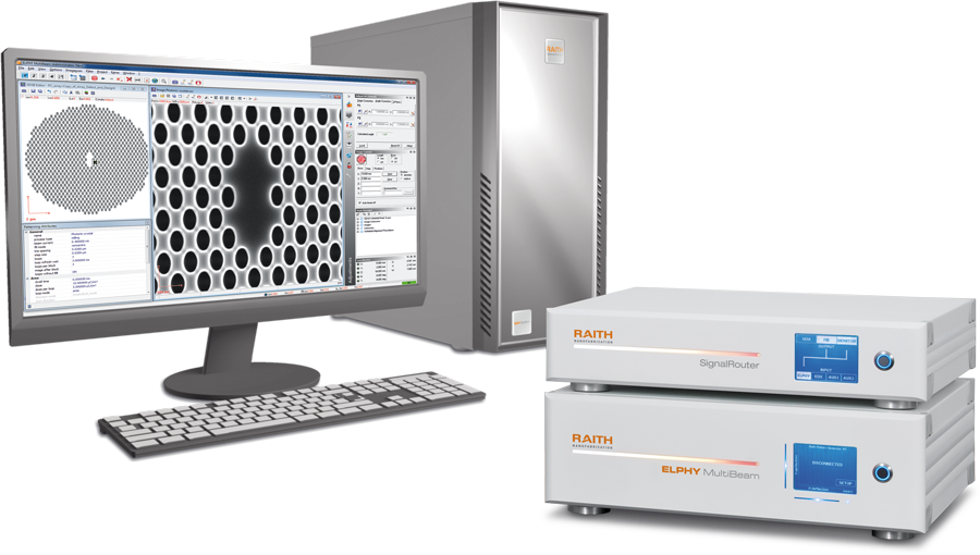
ELPHY at University of California Riverside
Jay LeFebvre
ELPHY at the University of California Riverside
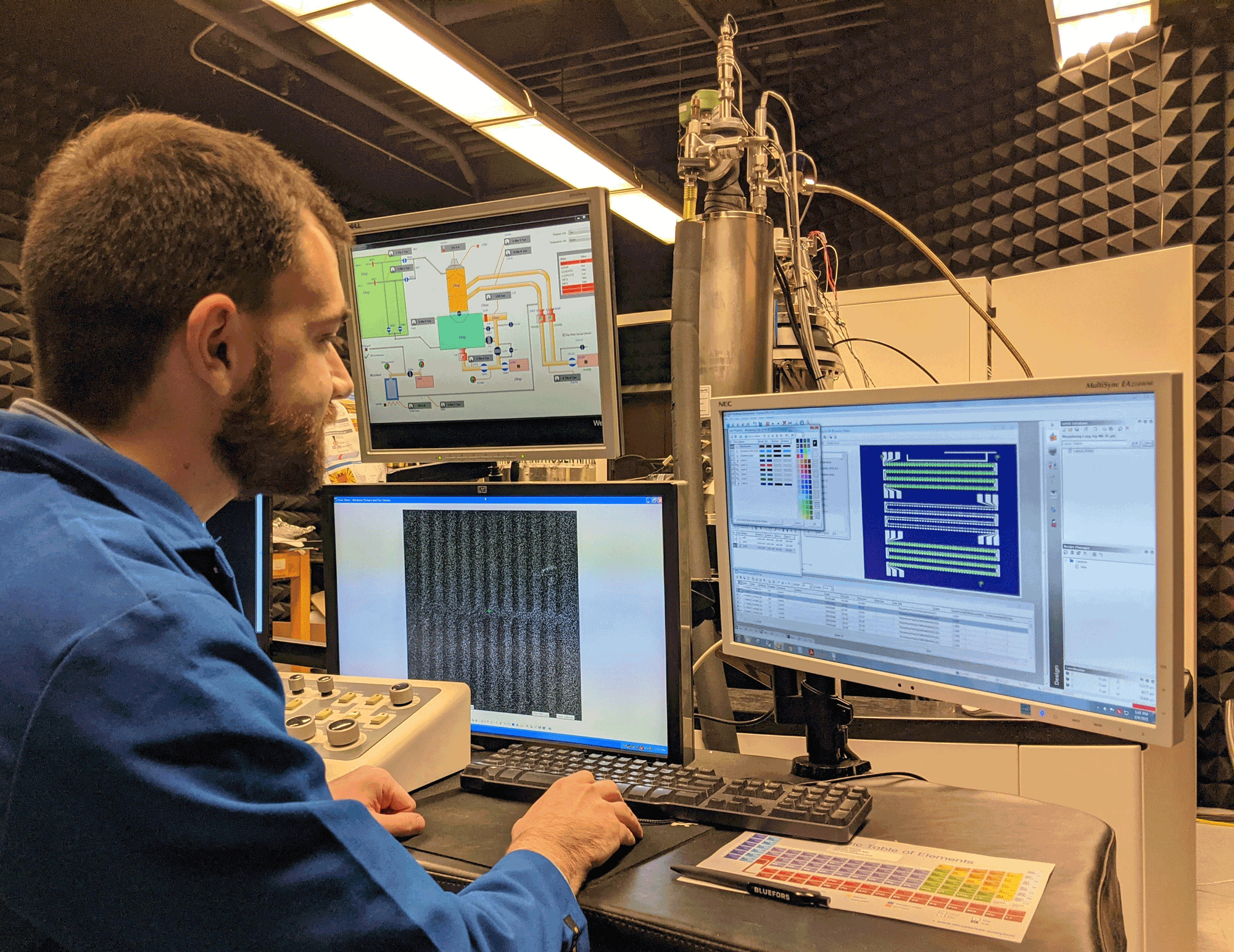
“Recently, the Oxide-Nano Electronics Laboratory (ONELAB) at the University of California, Riverside had the Raith ELPHY lithography add-on installed to a helium focused ion beam system (He-FIB). Commercial He-FIBs are being developed into promising tools for the advancement of nanotechnology, with applications in imaging, milling, resist exposure and deposition.
ELPHY provides us with the necessary lithographic functionality and control for patterning at the nanoscale with our commercial He-FIB system. After just one demonstration by the Raith team of the ELPHY system on our He-FIB, we were quickly developing automated He-FIB lithography at the millimeter scale while retaining consistent resolution at the nanoscale.
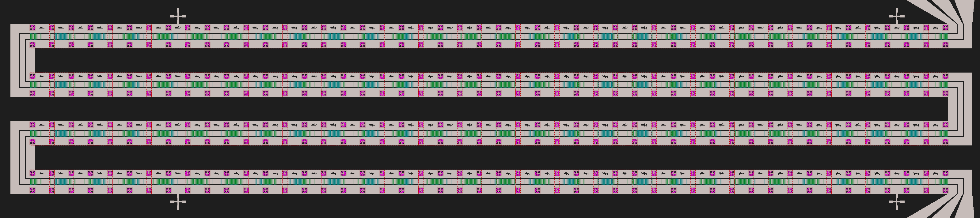
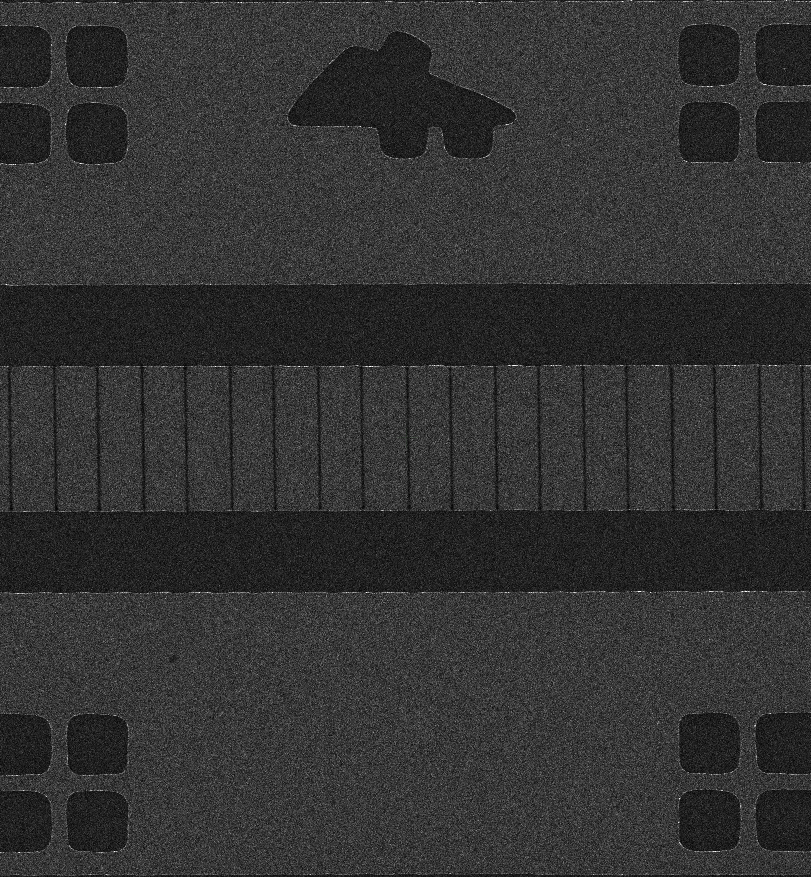
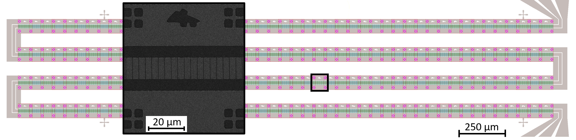
This functionality is critical for our research, as ONELAB’s principal investigator Shane Cybart pioneered the fabrication of high-quality, customizable Josephson junctions in high-critical temperature superconducting (HTS) electronics made from cuprate materials. The resultant devices are integral to the operation of revolutionary superconducting technologies, such as quantum limited sensors and advanced forms of computing. Josephson junctions are fabricated by having two superconducting bulk electrodes joined by a nanoscale non-superconducting barrier, typically a normal conductor or insulator. To create these barriers, we can take advantage of the material properties of cuprate oxides. These materials undergo a continuous superconducting to insulating transition under the irradiation of energized ions. He-FIB systems lend themselves readily to the fabrication of these barriers, as they can typically achieve an ion beam with 35 keV acceleration and a nanometer spot size, providing the ideal tool to selectively design and directly write Josephson junctions in HTS materials.
At ONELAB, we have developed an automated technique using ELPHY to directly write He-FIB junction arrays. We achieved ten times the number of junctions with minimal operator attention compared to previous manual techniques, all while maintaining uniformity at the smallest scales. To achieve nanolithography patterning across millimeter scales, ELPHY offers a variety of features including advanced batch-job automation to tune FIB beam parameters and stage control.
The installation of ELPHY on our He-FIB has greatly enhanced the complexity and dynamic range of our design capabilities. Raith produced a product that upgrades a research orientated tool, making it suitable for both industrial and academic purposes. It streamlines the fabrication process and allows users to focus more on innovation and less on the limitations of their instruments.”