Optoelectronics
Optoelectronic devices deal with light generation, light manipulation (e.g. modulation), and light detection (conversion of light into currents).
Optoelectronic devices are everywhere:
- displays,
- solar cells,
- data storage,
- sensing, and
- fiber-optical communication.
The latter field depends on semiconductor lasers (with special properties such as well-defined emission wavelength and high modulation rate), a field in which RAITH machines are well established. Furthermore, RAITH Electron Beam Lithography is especially used in R&D of advanced devices not yet in common commercial use, such as emerging quantum photonic devices.
From standard (DFB) lasers to non-standard lasers
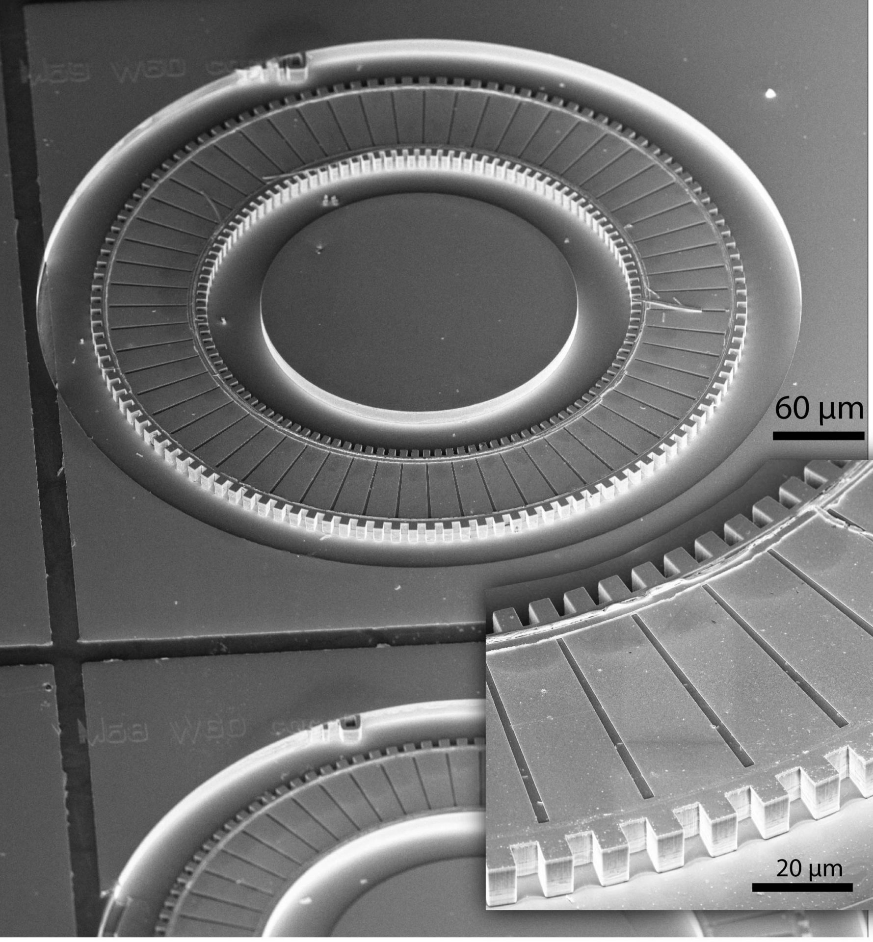
Raith machines (specifically the EBPG Plus and VOYAGER series) are widely used in mass production of (DFB) lasers (see DFB Laser section). DFB laser fabrication typically deals with linear laser cavities, and the feedback gratings are likewise straight-lined. The flexibility of RAITH electron beam lithography is showcased in non-standard devices such as ring lasers with radially arranged grating structures as shown in fig. 1.
This example shows that any (angle) orientation of feedback grating structures is possible. One application for the example shown is environmental monitoring in the mid-infrared band using an array of these ring lasers, forming a widely tunable spectroscopy source by tuning the individual ring lasers and switching on/off individual array elements.
Single photon sources for quantum photonics
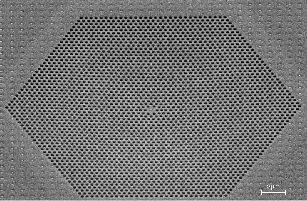
Continuous wave (CW) lasers emit a continuous stream of photons, while pulsed lasers emit pulses. Such lasers are typically designed with high average power in mind. Single photon emitters are different from these laser sources; they are of specific interest for quantum photonics (see quantum computing section). One approach to single photon emitters is a quantum dot embedded in a photonic crystal cavity. Fig. 2 shows an example.
An essential factor for the proper functioning of such an arrangement is the precise placement of the quantum dot structure relative to the photonic crystal slab, i.e. the electron beam lithography tool is required to have excellent overlay capability. Furthermore, the photonic crystal design parameters (like pitch or hole diameter) must be met with high fidelity. Reference 4 provides more insight.
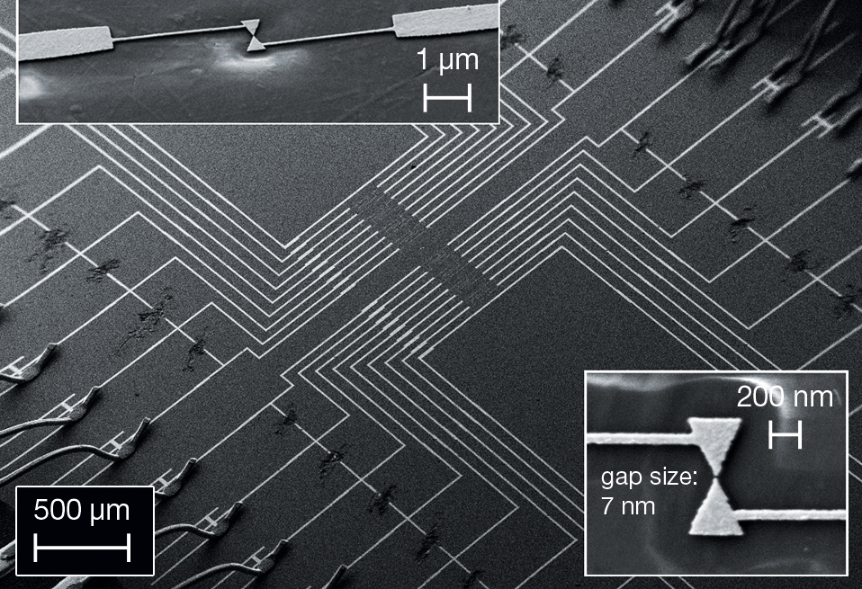
Photonic Integrated Circuits (PICs) for Quantum Optics
Light generation, light manipulation, and light detection could all or partly be integrated into a Photonic Integrated Circuit (PIC). The PIC shown in fig. 3 is quite special, comprising phase shifters and single photon detection functionalities for on-chip quantum optical experiments (further details are available in reference ¹). Bragg grating couplers (see Diffractive Optics section) are used to launch light (from external light sources) into planar waveguides on board the PIC (six Bragg grating couplers are visible in the lower part of the PIC in fig. 3).
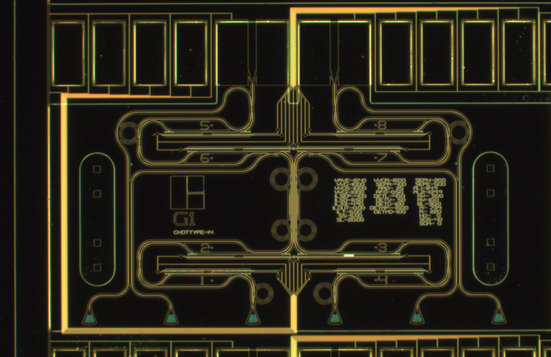
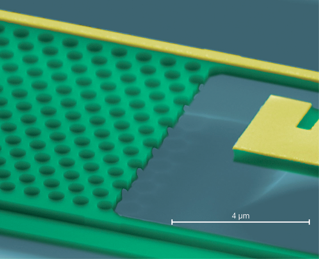
Fig. 4 shows a close-up of an electromechanical phase shifter as included in the device in fig. 3. This special phase shifter type is used to reduce the amount of dissipated heat. Electrostatic deflection of the nanofabricated mechanical structure changes the effective index of a nearby waveguide, resulting in a phase shift (which could be measured using a Mach-Zehnder interferometer on board the PIC) – after reference ².
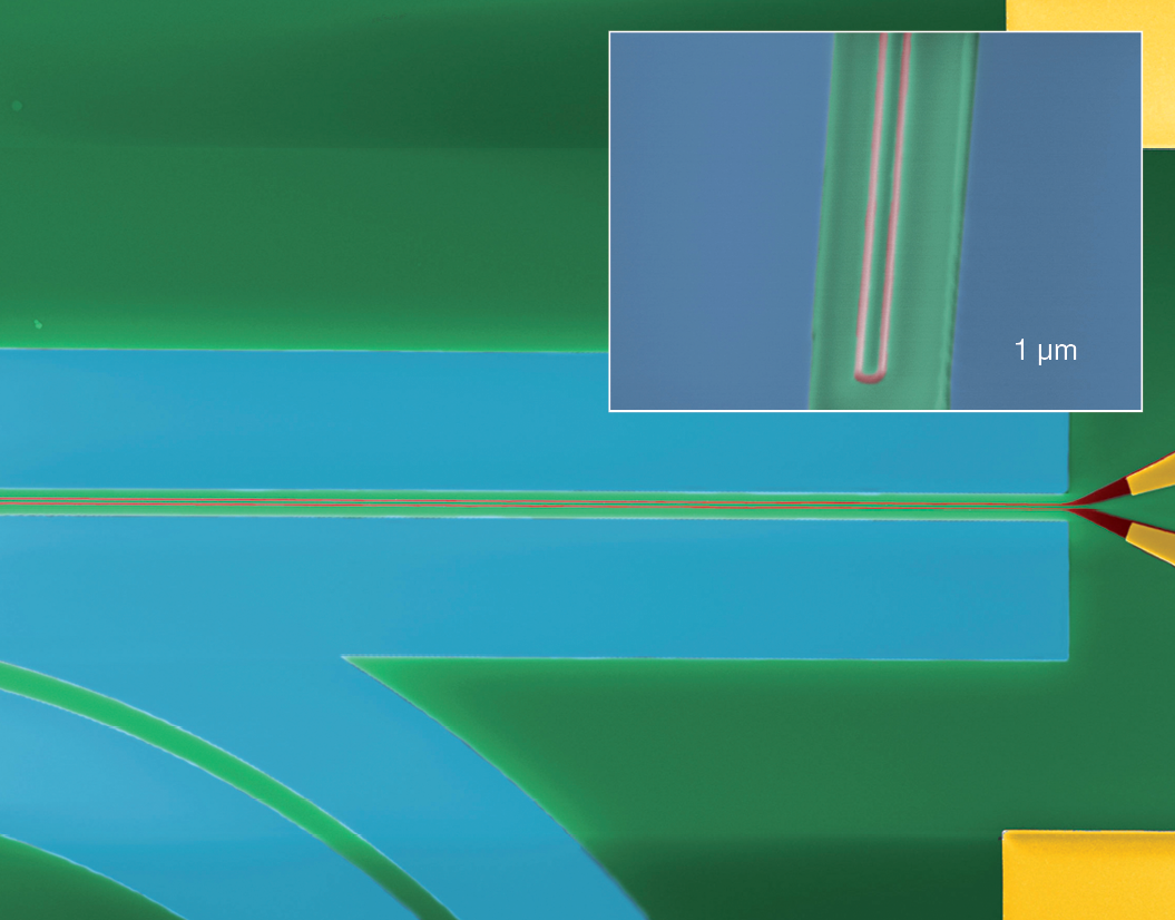
Quantum information processing and superconducting single-photon detectors (SSPDs)
Efficient integration of high-efficiency photon detectors in a PIC is extremely desirable in quantum optics. The circuit presented above in fig. 3 comprises integrated superconducting single photon detectors providing high quantum efficiency and ultra-fast response times (fig. 5).
The lithographer’s task is to make a U-shaped (NbTiN) nanowire with low width (e.g. 30 nm). A low nanowire width (along with a low thickness set by thin film deposition) is essential for proper functioning of the device. The geometrical layout of the detector could easily be optimized thanks to the flexibility of the patterning tool (here RAITH EBPG).
Waveguides and Photonic Integrated Circuits
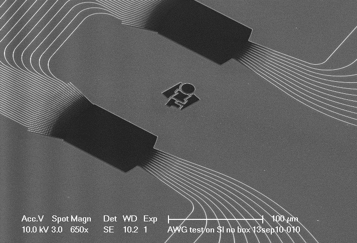
Photonic Integrated Circuits rely on high-performance waveguide structures. Given the size of real-world PICs (exceeding the single write field size available for patterning tools), several single write fields need to be stitched together. High-performance tools (like the RAITH EBPG Plus series) provide residual stitching errors in the range of 10 nm and below. Unwanted stitching artefacts could be further minimized or even completely eliminated using special integrated techniques. Many RAITH tools offer FBMS (fixed beam moving stage), a stitch-error-free writing mode used to make waveguides of highest quality, in addition to standard writing mode. Figure 6 shows an arrayed waveguide grating device (AWG) made using FBMS and a lithography tool that is typically affordable for academic environments (eLINE Plus).
Electrical Switching with Light
Fig. 7 shows an ultrafast optically gated electronic switch in which ultrashort laser pulses lasting for just a single oscillation period of light were used to drive ultrafast electronic transport. The nanoantenna shown uses plasmonic resonance to enhance the electric field of the light pulse. The electric field of the light pulses serves as an ultrashort bias to the antenna. The leads attached to the antenna branches enable the currents to be externally detected. Switching takes place on attosecond timescales! Details of the device physics are described in reference 3. Remarkably, electron lithography for this device was carried out using a SEM with attached pattern generator/software equipment “ELPHY” – affordable for university budgets and using only an existing TFE-SEM (with RAITH training provided alongside ELPHY installation on site).
Optoelectronics and Electron Beam Lithography Instrumentation made by RAITH
The selected applications above show a wide range of critical device dimensions ranging from the micron level down to the sub 10 nm level. The whole of this dimension range is covered by a single technology. But simply achieving dimensions is not sufficient to make a good device: “photonics needs accuracy,” as a recent article on silicon photonics stated. RAITH electron beam instrumentation has been proven to additionally provide accurate placement of device elements with respect to each other, and boundary and dimension control of elements over larger areas.
“I can easily achieve the required dimensions using optical lithography” is true in many (but not all!) cases, but the statement must often be continued: “using very advanced CMOS-node factories.” In practice, RAITH tools are regarded as more universal and affordable for the research community, especially at universities. And even well-funded industrial R&D, when suffering from excessively long development cycle times, benefits from the use of RAITH tools to speed up its pace and to work on devices beyond the scope of optical lithography.
REFERENCES
[1] RAITH Application note “Photonic circuits for on-chip quantum optics” (available as download here)
[2] M. Poot and H. X. Tang, Broadband nano-electromechanical phase shifting of light on a chip, Appl. Phys. Lett. 104 061101 (2014)
[3] Nature Photonics 10, 667–670 (2016) doi:10.1038/nphoton.2016.174; Tobias Rybka et al, Sub-cycle optical phase control of nanotunnelling in the single-electron regime;
https://www.nature.com/articles/nphoton.2016.174
[4] M. Schatzl et al., Enhanced Telecom Emission from Single Group-IV Quantum Dots by Precise CMOS-Compatible Positioning in Photonic Crystal Cavities; http://pubs.acs.org/doi/pdfplus/10.1021/acsphotonics.6b01045