Webinars
To learn about new technologies, trends and opportunities in the nanoworld is the objectives of our webinars. We want our customers to learn about new developments in electron beam lithography, FIB-SEM nanofabrication and large-area imaging / reverse engineering.
Upcoming Webinars
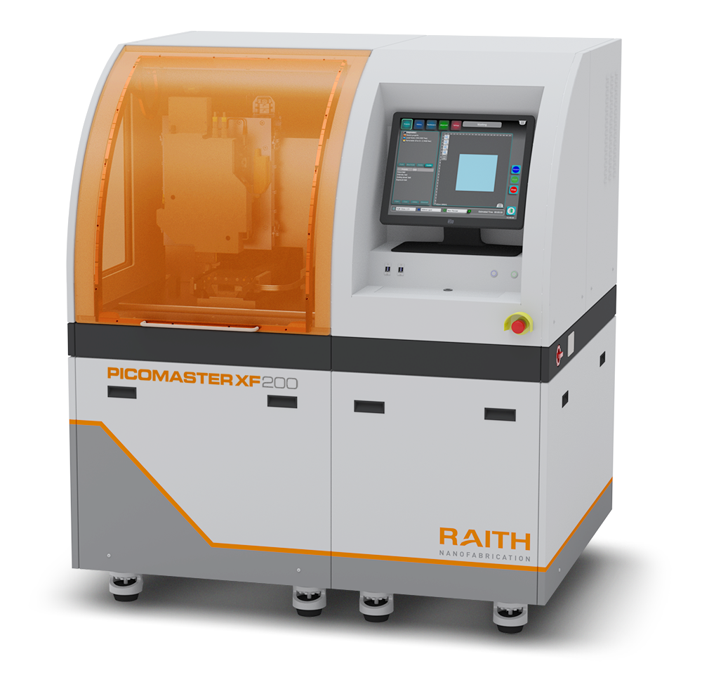
Mastering Nanostructures - Raith's Laser Lithography Unveiled
An easily exchangeable optical module, non-stitching writing strategies and a hybrid autofocus are only some of the features that will take your laser lithography to the next level.
Register for our webinar and find out, how the PICOMASTER enables high-resolution results with a high aspect ratio, uniform structures over a full wafer, outstanding performance even in thick resist and much more.
To cater the different time zones we will over the webinar at two times. Simply choose the one that better fits your schedule.
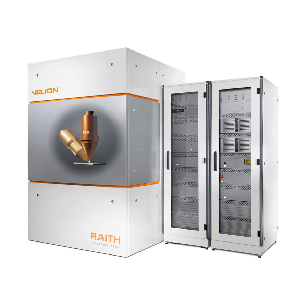
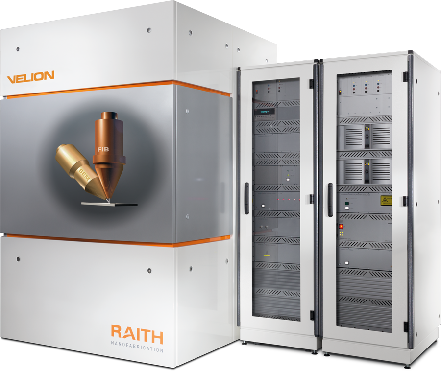
VELION – FIB-SEM for nanofabrication beyond limits
Raith has been continuously driving developments in FIB nanofabrication and consistently been implementing new technologies to refine processes and enable cutting-edge science and research. Automation, long-term stability and highest accuracy in placement along with innovative technologies such as Liquid Metal Alloy Ion Sources (LMAIS) have also made an important contribution to the maturity of the VELION to take FIB-SEM to the next level for nanopatterning and making VELION the ideal companion for machine driven nanofabrication.
In this webinar we will be presenting VELION FIB SEM and related applications.
To cater the different time zones we will over the webinar at two times. Simply choose the one that better fits your schedule.
The next generation FIB source - GaBiLi for 2D and 3D ion microscopy
Liquid Metal Alloy Ion Source (LMAIS) is a Focused Ion Beam (FIB) source technology that has been established for nanofabrication over the last years. Most recently, Lithium ion imaging with from GaBiLi eutectic alloy at sub 2nm lateral resolution has become feasible.
In this webinar we will be introducing the GaBiLi FIB source and associated workflows for stable 3D tomography without sample tilt by Bismuth milling and intermittent Li imaging.
To cater the different time zones we will over the webinar at two times. Simply choose the one that better fits your schedule.
On-Demand Webinars
Webinar PICOMASTER
With the addition of the PICOMASTER series to our portfolio, we are now offering solutions for laser lithography as well. In the webinar our colleagues Marc Ujma and Viacheslav Vlasenko will introduce our new laser lithography solutions and show you how to create high resolution features at rapid speed!
Find out how innovative writing and exposure strategies will take your lithography to the next level and watch the webinar.
Mastering Nanostructers – Raith’s Laser Lithography Unveiled
An easily exchangeable optical module, non-stitching writing strategies and a hybrid autofocus are only some of the features that will take your laser lithography to the next level.
In this webinar we introduce the the PICOMASTER and show you it enables high-resolution results with a high aspect ratio, uniform structures over a full wafer, outstanding performance even in thick resist and much more.
Webinars VELION - A Novel FIB-SEM Nanofabrication Instrument Concept and its Applications in Nanoscale Science and Engineering as well as Ion Microscopy
Raith has developed advanced Focused Ion Beam instrumentation over the last fifteen years with the vision that nanofabrication has special requirements that should drive the development of FIB technology. As a result, the VELION was developed to pave the path for unique applications in nanofabrication.
In this webinar series we will show you the unique capabilities for large area patterning as well as employing ion species beyond gallium to enable numerous applications in the field in nanoscale science and engineering as well as ion microscopy.
Next Generation FIB source GaBiLi for 2D and 3D ion microscopy
The VELION FIB-SEM is a powerful nanofabrication system. With it’s top down multi ion FIB from LMAIS on a 4 inch laser interferometer stage cutting edge application become possible. In this webinar we introduce the general VELION setup and present cutting edge application results.
Explore unlimited process pathways with VELION FIB-SEM for direct patterning of smallest features over large areas at highest precision and stability. We will cover applications in the fields of ion implantation, large area FIB nanofabrication, high precision patterning on the wafer scale and 3D direct milling.
Next Generation FIB source GaBiLi for 2D and 3D ion microscopy
Liquid Metal Alloy Ion Source (LMAIS) is an established FIB source technology for nanofabrication that provides versatile solutions for nanofabrication and imaging. The combination of Gallium, Bismuth and Lithium (GaBiLi) enables new approaches for 2D and 3D ion microscopy.
The webinar introduces the GaBiLi source and it’s usage for high resolution, low damage ion microscopy. It explains how a mature nanofabrication system was converted into a powerful ion microscope and enables applications such as 3D tomography without sample tilt.

Webinars EBL and metrology
In this webinar series we will cover different aspects of electron beam lithography such as relevant performance parameters, large area imaging, 1D and 2D materials, metrology and many more.
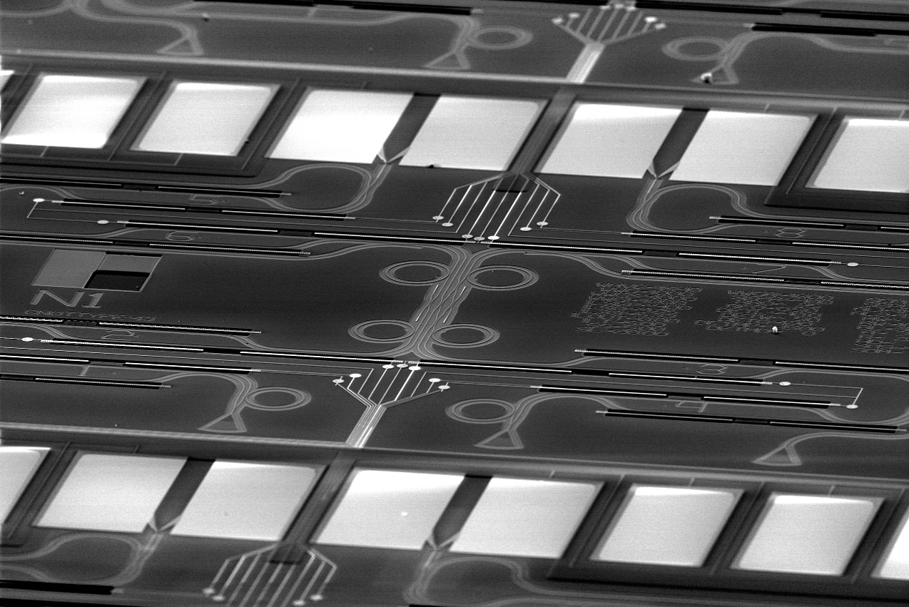
Relevant Performance Parameters for professional EBL: About Truth and Myth
In the nanofabrication market, there is a wide choice of electron beam lithography systems, each having specific strengths for specific applications. These EBL systems are typically categorized by their main specifications and performance parameters somehow representing their lithographic capabilities with respect to throughput, accuracy or resolution. In this webinar, the nature of and the interplay between these main parameters such as beam energy, beam current, beam diameter, write field size, pattern generator speed, stitching or overlay values and their relevance for a good system performance with respect to specific applications is addressed.
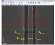
Nanocontacting and Device Fabrication of randomly distributed 1D and 2D materials
1D and 2D materials are attracting more and more researchers to develop future electronic devices and sensors. Such materials can be nanowires, -tubes or -whiskers, flakes or growing islands of CVD materials. Typically their distribution on the chosen substrate is random. Representing a very common EBL application, in a first step it is most important to identify and contact these nanostructures in order to connect them to the outside macroscopic world for fundamental analysis such as e.g. conductivity measurements. Alternatively or in subsequent process steps respectively, these low dimensional nanostructures need to be turned/integrated into a functional device. In this webinar, some alternative approaches for identifying, nanocontacting or integrating randomly distributed 1D and 2D materials – even in semi-automated way over large areas and by maintaining pristine surfaces – are presented.
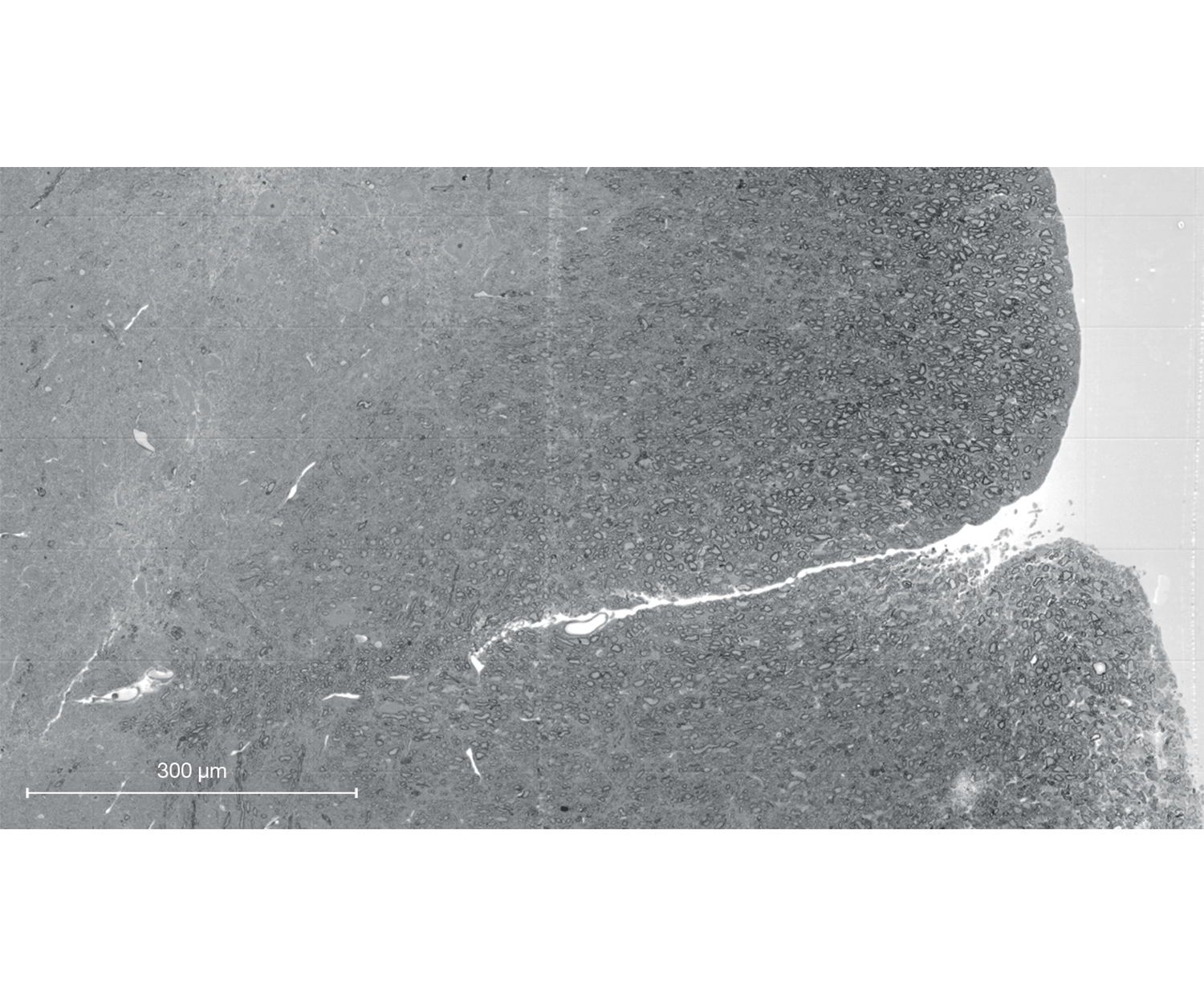
Nanodevice Optimization by automated large Area Imaging and Metrology
Typically, nanodevice fabrication requires a few electron beam lithography exposure steps and related optimization loops in order to achieve a functional device “perfectly” matching required dimensions and quality. A common procedure is to expose a matrix of the nanostructures in many different writefields and play around with various parameters such as exposure dose or patterning strategy from one writefield to the next. Subsequently, the results need to be inspected and qualified in a dimensionality check. This may happen by subsequent acquisition of a series of SEM images for further evaluation or direct metrological measurements at the places of interest, alternatively. In this talk, various approaches for qualitative inspection and quantitative metrological measurements are presented in order to improve the nanodevice quality during the device optimization process.
Webinars VELION - A Novel FIB-SEM Nanofabrication Instrument Concept and its Applications in Nanoscale Science and Engineering
Raith has developed advanced Focused Ion Beam instrumentation over the last fifteen years with the vision that nanofabrication has special requirements that should drive the development of FIB technology. As a result, the VELION was developed to pave the path for unique applications in nanofabrication.
In this webinar series we will show you the unique capabilities for large area patterning as well as employing ion species beyond gallium to enable numerous applications in the field in nanoscale science and engineering.
Focused Ion Beams for advanced nanofabrication
The VELION is a FIB-centric FIB SEM where the ion beam is always perpendicular to the sample plane. With a side mounted FE-SEM column and a laser interferometer stage at nm accuracy more sophisticated applications become possible. The VELION takes advantage of stability, large and fully corrected fields-of-view, and laser interferometer stage. These demands and features are essential components in EBL instrumentation and have been utilized in a FIB SEM system for the first time. In this talk we will introduce the general setup of the VELION, the instrument concept in order to serve needs for advanced nanofabrication. The plasmonics and nanophotonics community has already demonstrated that there are applications whereby FIB on a Lithography platform has its advantages in delivering answers to important questions in nanoscale science and engineering.
FIB SEM applications beyond gallium and benefits of AuSi ion beams
With the appreciation that the ion’s properties can have dramatic consequences on the physical and chemical nature of the resulting nanostructures, we have extended the technology towards the stable delivery of multiple ion species selectable into a nanometer scale focused ion beam by employing a liquid metal alloy ion source. This LMAIS provides single and multiple charged ion species of different masses, resulting in significantly different interaction mechanisms. In this talk we also discuss the motivation behind applications employing non-Gallium species, such as Silicon, Gold, Germanium and their benefits and present results of Au and Si ion beam nanofabrication.
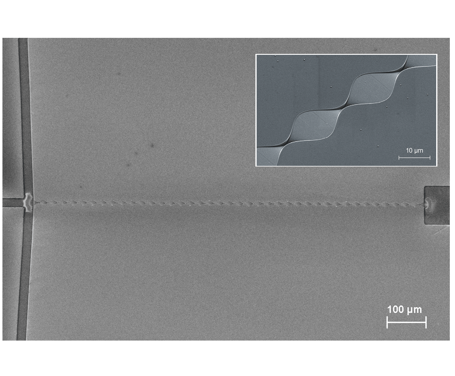
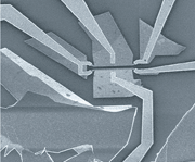
Advanced FIB patterning and Large Area applications
Ion beam nanofabrication has proven unique strengths by numerous applications in R&D prototyping. It helps to achieve scientific results by in-situ optimization of patterning parameters for 2D and 3D structures. Traditional ion beam-based instruments lack large, corrected fields-of-view and laser interferometer stages, which are essential components in EBL instrumentation and are mandatory for accurate ion beam nanofabrication. Here we present FIB patterning of large photonic devices like extended photonic crystals and mm-long waveguides. To overcome FIB milling related patterning artifacts like edge effects at stitch field boundaries, advanced strategies have been developed. Sophisticated continuous stage movement modes as FBMS (Fixed Beam Moving Stage) for extended continuous trench milling and MBMS (Modulated Beam Moving Stage) for stitch free patterning of periodic elements are demonstrated as well with the help of real time SEM live imaging movies of ion beam milling employing these modes. Furthermore, we present examples of advanced FIB nanofabrication by making use of the outstanding long term stability of the nanoFIB column and accuracy of the laser interferometer stage.
Other webinars
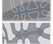
Wafer Scale Device Fabrication And Electrical Characterisation For Graphene & 2D Materials
This webinar is giving you an overview of wafer-scale device fabrication and characterization technologies that would drive development of graphene and 2D materials based technology to the next stage of technology readiness. Three different aspects of graphene/2D device development work are covered, i.e., materials fabrication, lithography and non-destructive electrical characterisation
This webinar was delivered in conjunction with Oxford Instruments.
Perfecting Large Area, High Resolution SEM Imaging with 3D-Stitching
This webinar explains how the combination of the resolution and flexibility of an SEM with the stability and automation of an electron beam lithography system can help solve issues with throughput and stitching errors that are often associated with large area, high resolution SEM image applications in semiconductor reverse engineering, material science and life science (e.g. connectomics).
This webinar was delivered in conjunction with Microscopy & Analysis.
Symposium on the fabrication and sensing of well-designed quantum devices
This symposium was organized with Delmic, Oxford Instruments, and Qnami to share comprehensive knowledge about the fabrication and sensing of well-designed quantum devices! Experts and customers from the participating companies will describe how the technology allows engineering of quantum devices by controlling the size of the nanomaterial with nanometer resolution.