Nanophotonics
In nanophotonics, material is structured at the nanoscale in order to create new optical properties for a large variety of applications. Prominent examples of commercial nanophotonic devices are diffractive optical elements (DOEs) (including Fresnel lenses and blazed gratings) or distributed feedback lasers (DFB).
- photonic crystals,
- photonic metamaterials, and
- plasmonic elements.
Related structures typically comprise feature dimensions from about wavelength periodicity down to nm scale.
All the optical materials mentioned above affect light propagation in specific ways.
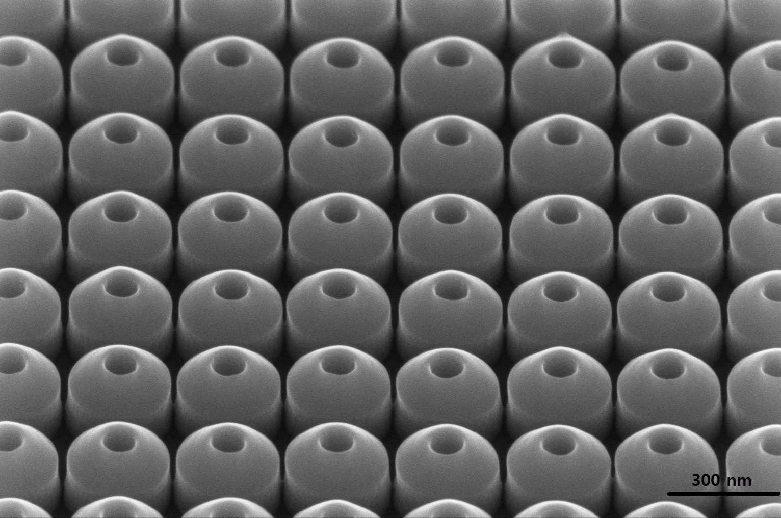
In photonic crystals, periodic optical nanostructures result in photonic bandgaps equivalent to electronic bandgaps in crystalline material. The resulting optical properties, where certain optical waves are not propagating, are used in applications including optoelectronic devices.
Some vertical-cavity surface-emitting lasers (VCSELs), for example, use metasurfaces in the form of sub-wavelength gratings on the laser emission window. The top surface gratings develop birefringence effects, which, as a consequence, lead to laser mode selection in VCSELs for certain modes with specific light polarizations. The active zone design, the distributed Bragg reflector, and the top grating structure in modern VCSELs together form a complex nanoscale laser system, which needs to be built with the highest precision.
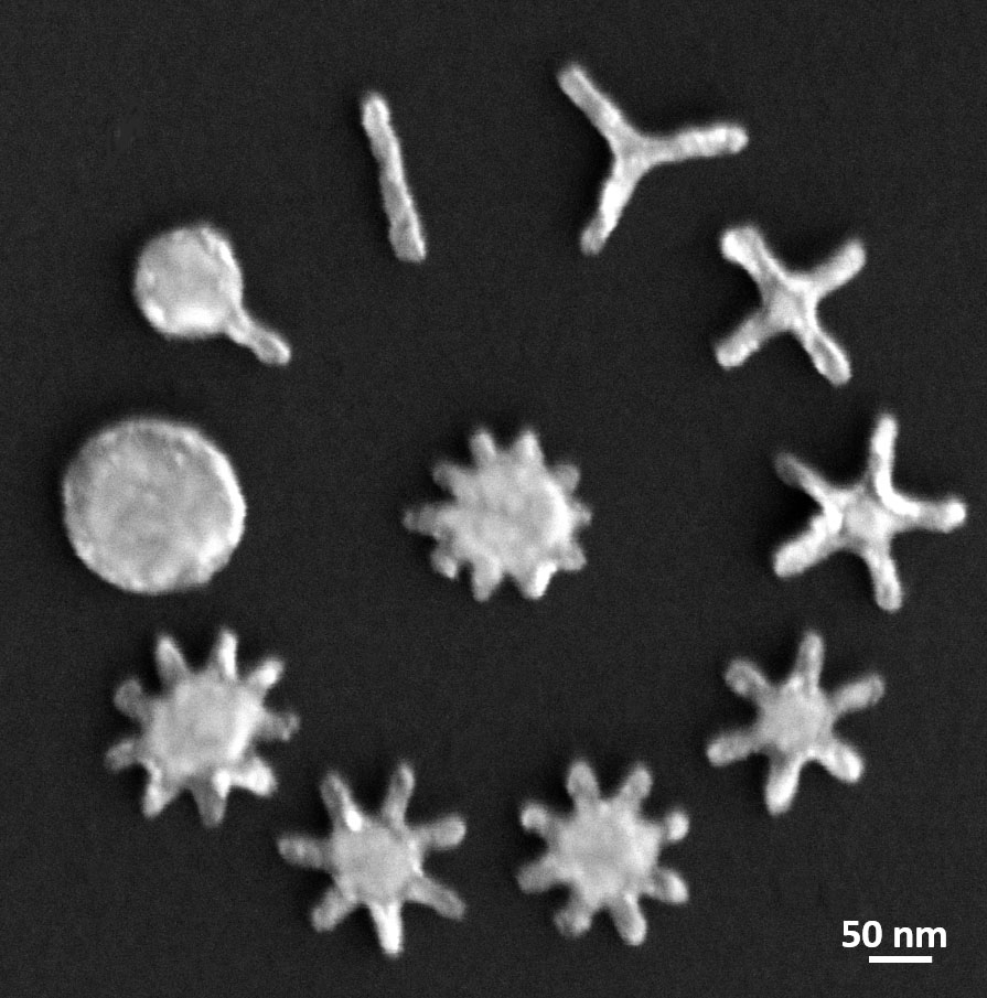
A further exciting, and quickly expanding, area in nanophotonics where significant research activity is taking place is the field of plasmonics. Plasmonics deals with surface plasmon resonance (SPR), where light interacts with dielectric/metal interfaces. It has a wide range of applications in areas such as biosensorics, optical data transfer, or even innovative photovoltaic cells. Plasmonic structures could be as simple as metallic nanoparticles, or as complex as structured nm shapes with well–controlled critical dimensions. Non-classical plasmonic light propagation in combination with advanced nm–scale device structuring capabilities provided, for example, by electron beam lithography (EBL) offers great opportunities to design innovative devices for various applications.
In general, nanophotonics is still a very dynamic field of development and research. Advances in distortion–free, precise nm–scale patterning of large areas utilizing EBL are fueling both nanophotonic research and device fabrication.
Charged particle lithography in nanophotonics
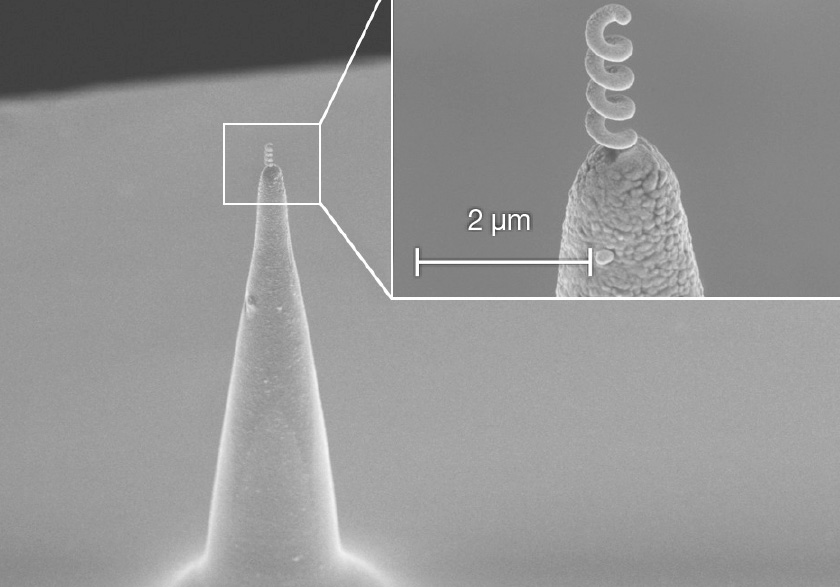
Charged particle lithography comprises EBL on the one hand and focused ion beam (FIB) techniques on the other. In EBL patterns are transferred into material through a resist-based lithography process, while FIB lithography is used for direct write structuring. EBL is typically significantly faster than FIB-based patterning and is therefore the method of choice for manufacturing and research whenever speed or large-area exposure are critical. FIB based patterning, on the other hand, offers the flexibility of direct write patterns on various substrates. It even offers unique 3D capabilities in a single run without having to apply grayscale lithography processes. A common requirement for both EBL and FIB patterning methods is the need for precise beam control in combination with high-precision sample navigation.
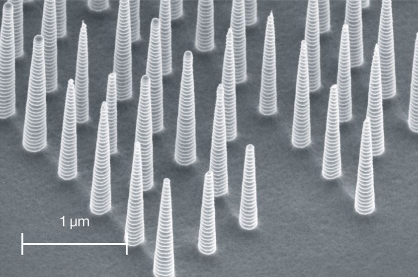
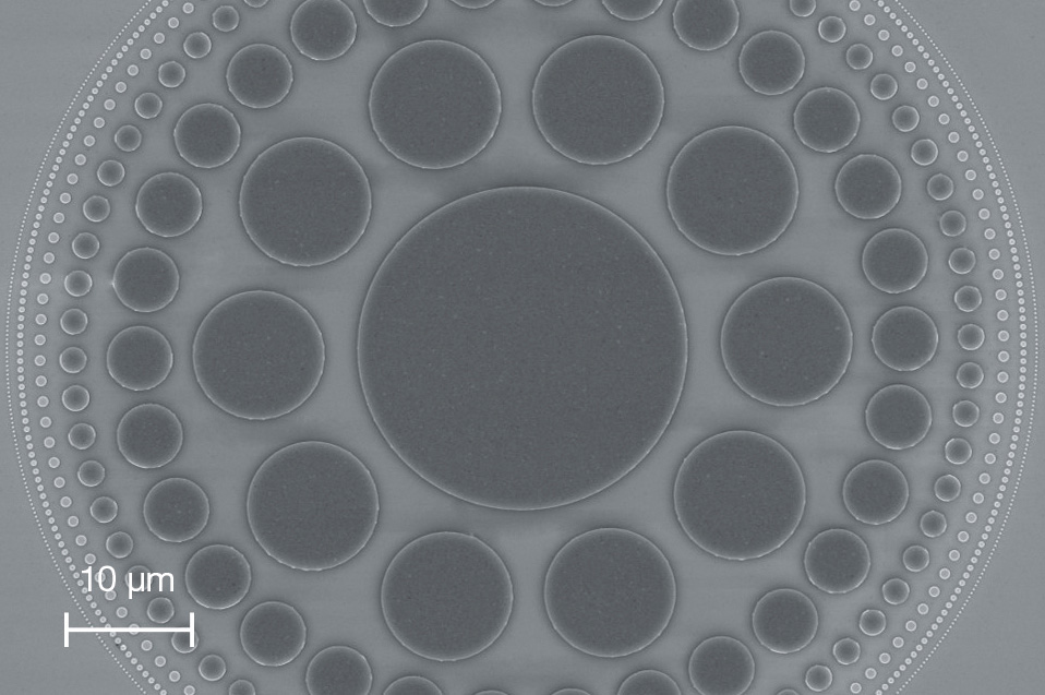
The nature of diffractive optical elements requires excellent feature definition at the nm scale with low line width roughness (LWR), but also distortion-free large-area patterning. Both demands are essential for nanophotonic devices to achieve high performance. As a consequence, high-end EBL systems for nanophotonics provide distortion-free large-field patterning with high beam resolution and excellent field stitching performance. For FIB-based systems, where write cycles are slower compared to EBL, drift-free sample stages and a stable ion current are mandatory. In addition, many applications in FIB patterning require Ga-free milling to avoid sample contamination
Photonic Integrated Circuits
In addition to the previously mentioned DOEs, photonic integrated circuits (PICs) constitute a further hot topic in nanophotonics today. PICs builds on the principles and the technology of semiconductor electronics, where two or more optical elements are combined on a single chip. Integration of these optical elements on a single substrate allows researchers and engineers to combine various functionalities in the area of data communication, sensoring and life science.
The PIC principle is scalable: typical optical elements such as waveguides, photonic sensors, and optical fiber interfaces can be combined in specific ways in order to obtain optimized or new device functionalities. Compared to electronic IC history, PIC development is a much younger discipline, exhibiting a huge innovation potential. Among the large variety of different PIC material systems, the two most popular semiconductor material systems for PICs are indium phosphide (InP) and silicon-based photonics.
InP is a direct bandgap compound semiconductor material commonly used in high-power, high-frequency optoelectronics. InP-based PICs include light generation and amplifying functionality, light modulation and passive elements such as waveguide structures. Low-optical-loss InP PIC devices are deployed in applications including high-frequency, long-distance telecom transmitters.
In contrast, the high interest in Si-based PICs is not related to the optical material properties which comprise an indirect bandgap. Here, the interest is driven much more by the availability of well-established leading-edge processing capabilities, developed over decades by the silicon industry with its enormous engineering power. The opportunity to utilize this high-volume, low-cost manufacturing infrastructure is well suited for large-scale deployment of silicon photonic PIC devices. One or two decades ago, the introduction of silicon-on-insulator (SoI) technology and SiGe processing on Si chips turned into well-established and robust technologies which today boost the optical properties of silicon photonic elements.

In high-volume manufacturing, a cost-efficient method of device development with short development cycles is crucial for meeting time-to-market requirements and therefore ensure commercial success. EBL– and FIB-based lithography systems, with their unique capability of providing fast and flexible maskless patterning, are powerful tools for speeding up development in silicon photonics in particular and for driving innovation in nanophotonics in gereral.
- artifical intelligence in nanotechnology
- graphene applications
- nanotubes
- nanoelectronics
- nanotechnology in material science
- fundamental research in nanophysics
- ion-beam-induced deposition
- electron-beam-induced deposition
- TEM lamella preparation
- atom probe tomography
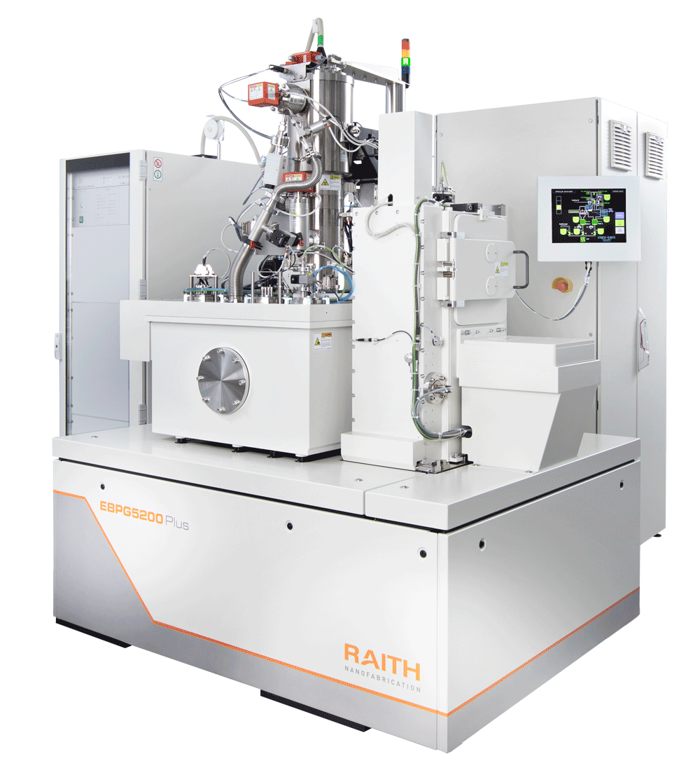
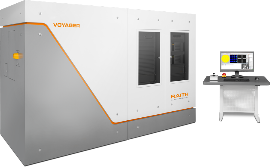
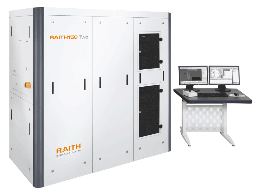
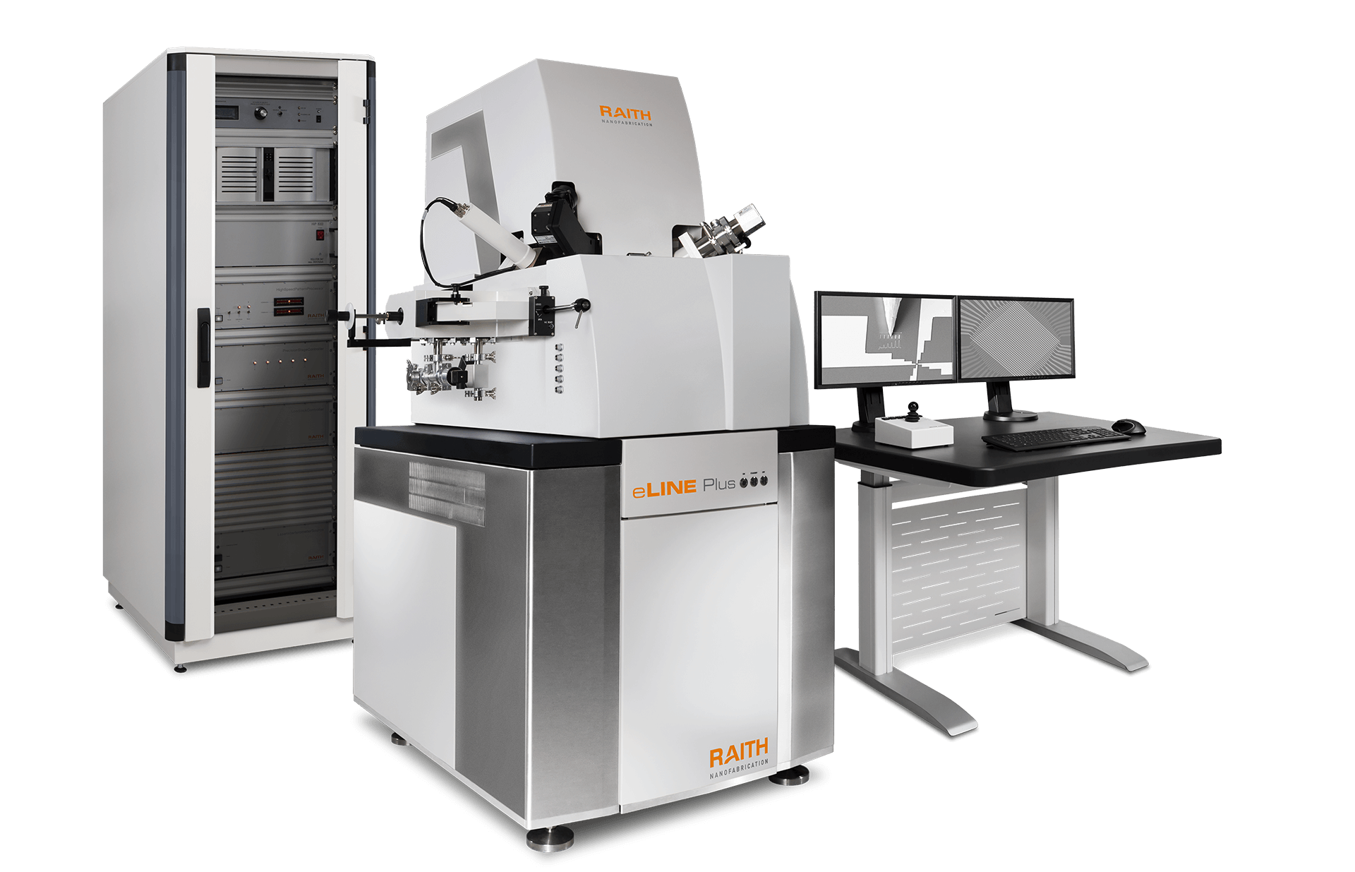
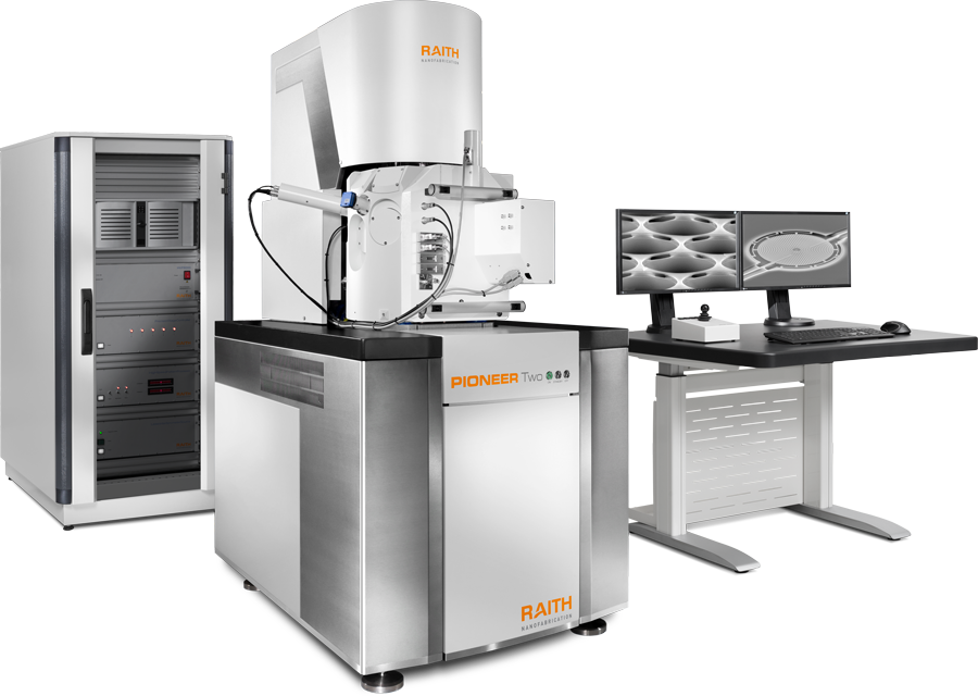
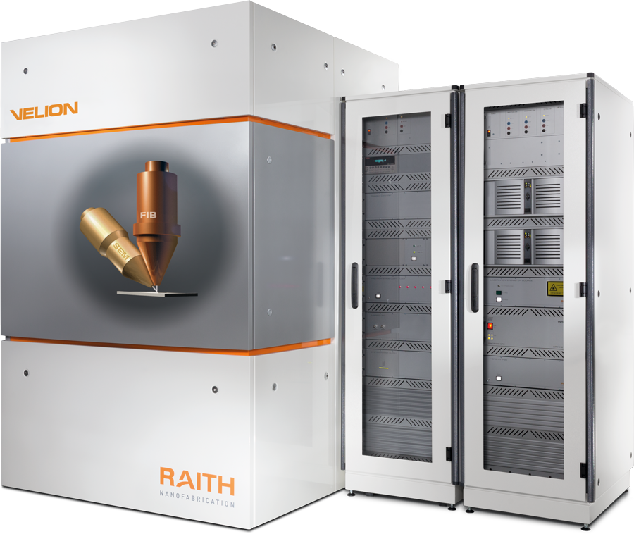
Our solutions for patterning in nanophotonics
Maskless high-precision, high-resolution EBL- and FIB-based patterning systems offer high flexibility for precise and robust nm-scale patterning of nanophotonic devices on a large set of different materials. Raith offers the whole range of Gaussian beam lithography instruments, from highly versatile patterning SEMs to dedicated leading-edge EBL systems. Raith’s product portfolio is complemented by Ga-free FIB-based structuring for rapid prototyping and versatile high-precision patterning on established and unique material substrates. In the innovative area of nanophotonics, requirements for structuring new devices with highest precision might be demanding. We encourage you to consult Raith when you are seeking specific solutions or whenever you need further information on our lithography equipment for nanophotonics. We look forward to receiving your inquiry.