Integrated Circuit Analysis
Integrated circuit analysis covers many different applications, mainly within the semiconductor business. Analysis may be performed for certain properties, quality criteria, or IP (intellectual property). The semiconductor manufacturing process typically distinguishes between electrical and physical analysis. Raith’s reverse engineering/SEM solution focuses on physical IC analysis.
Physical properties that are often analyzed by metrology are
- CD (critical dimension),
- distances, particles,
- chemical properties, and
- physical connections (shorts or opens).
In integrated circuit analysis the goal is to extract an optical image of the code used on a given chip and then analyze the chip accordingly, depending on different approaches and reasons.
Reverse engineering departments at semiconductor companies or RE service laboratories are mainly interested in analyzing netlists and electrical schematics to find or exclude copyright–protected elements. Chip manufacturers often include a certain pattern without functionality in their design; the presence of this pattern on a competitor’s chip can be proof of copyright violation.
Another approach is the currently strongly growing field of cybersecurity. As chips are often produced by third-party manufacturers, IP owners have to identify and exclude hardware trojans in their ICs to be able to guarantee safety to their customers.
And finally, IC analysis is of interest in the obsolescence business. Spare parts are often needed for old hardware items which are no longer produced. Integrated circuit analysis then helps to extract the complete mask data for all relevant layers from packaged ICs as a basis for spare part reproduction.
The best solution for resolution, accuracy, and stability in IC analysis
Tools for the above-mentioned applications must primarily provide
- highest resolution,
- ultra-high positioning accuracy,
- high position stability for long-term applications,
- powerful image processing,
- a variety of detectors,
- and certainly a user-friendly GUI/UX
- with the highest possible level of automation.
All these properties overlap with the requirements for the nanofabrication systems that Raith has supplied since the 1980s. Irrespective of the type of charged particles our systems use, they all share highest-resolution electron or ion optics, laser interferometer-based stages, drift optimization (e.g. passive and active temperature stabilization), multiple detectors (e.g. in-lens BSE, post-lens BSE, ET-SE2, in-lens, EDS,…) and a powerful and widely accepted software platform. This platform focuses on image acquisition/processing and automation as well as on writing nanostructures.
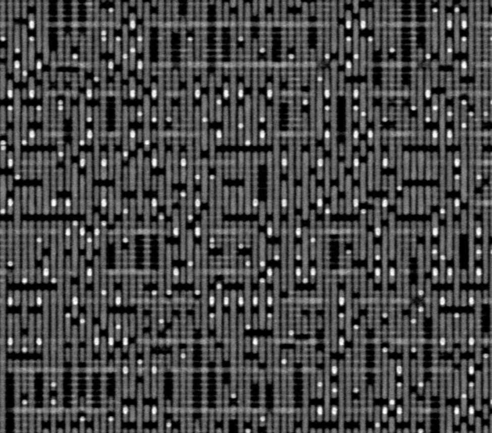
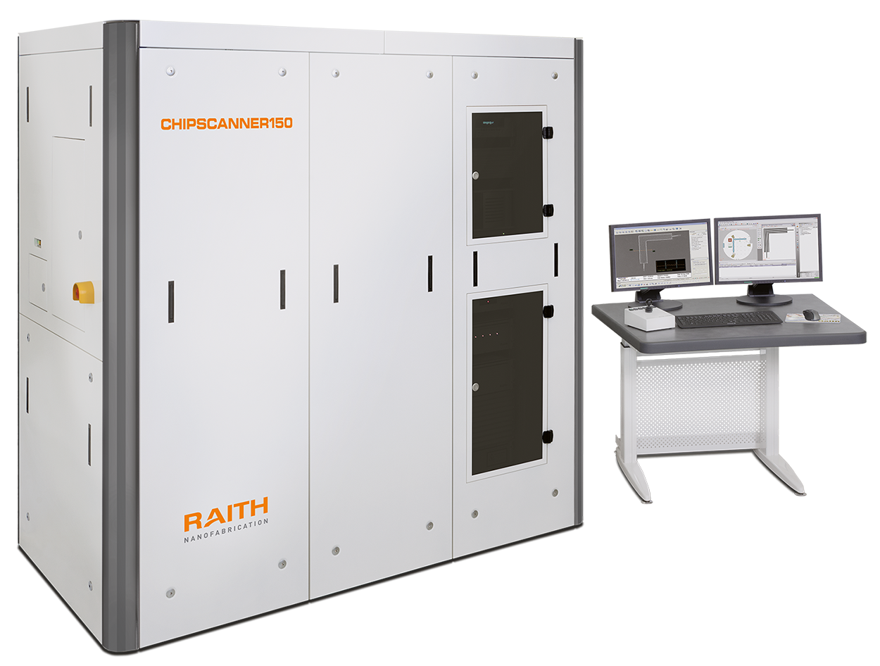
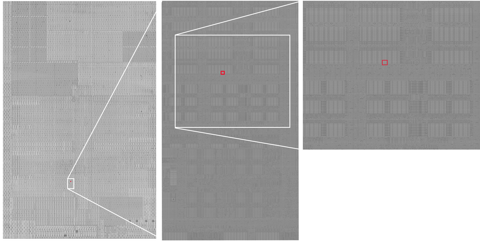
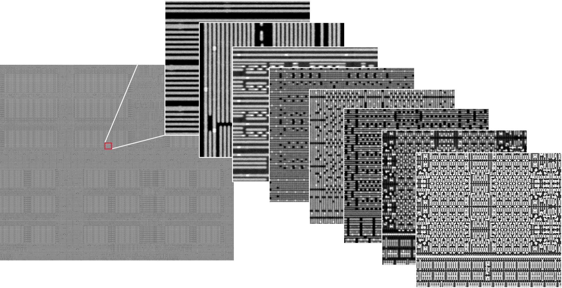
Moreover, Raith’s CHIPSCANNER makes use of the lithography platform and turns its proven capabilities into a 3D SEM imaging solution. While traditional SEM instruments are usually limited by small, uncalibrated fields of view (FOVs) and do not offer precise sample positioning, Raith’s CHIPSCANNER provides a solution for scanning surfaces up to cm² areas with nm resolution and excellent layer-to-layer accuracy, and therefore for the precise layout extraction or 3D modeling needed in integrated circuit analysis.
IC reverse engineering and process control
While integrated circuit analysis is a huge field, the main applications in which Raith customers work are reverse engineering (RE) and process control (quality control).
In reverse engineering the focus lies in reconstructing the underlying structure of a given chip for the purpose of copyright protection or reconstruction of spare parts.
Process/quality control focuses on chip analysis with the goal of identifying potential malware or problems/errors within the chip.
Our solutions for integrated circuit analysis
For RE, customers Raith offers complete solutions from high-speed large-area image acquisition with nm stitching accuracy up to automated CAD extraction and even optional netlist extraction. Our Laser Interferometer Stages and powerful software extensions enable CHIPSCANNER to offer the most accurate and complete reverse engineering solution available worldwide. With application-specific options such as nanomanipulators for electrical measurements, EDS for chemical analysis, and many more, CHIPSCANNER is a dedicated solution for IC analysis.
For metrology purposes we offer systems similar to a CD-SEM, slightly less automated but more flexible and with much lower COO (cost of ownership). In-image measurements are possible, as is long-distance metrology over the full travel range of our system stages (up to a few inches). Powerful software algorithms support a variety of measurements and statistics. All Raith turnkey systems are equipped with these functions and are especially suitable for occasional use of the metrology function.