Quantum Technology
Quantum technology is a quickly emerging field in physics and engineering whereby new devices are based on quantum mechanics, rather than classical physics. Quantum technology devices make use of the principles of quantum mechanics, like superposition and entanglement. The most popular applications include:
- quantum sensors,
- quantum cryptography,
- quantum communication, and, most recently,
- quantum computing
Quantum communication offers a perfectly secure method of communication by using entangled quantum states for data transmission. The current aim is to build a secure quantum internet by protecting information channels against eavesdropping using quantum cryptography based on quantum key distribution.
Quantum computing holds promise to vastly accelerate computation by using qubits (quantum bits) instead of digital bits (classical bits). Superposition and entanglement in qubits enable massive parallel computing in quantum computers. Quantum algorithms with qubits could allow computation of specific tasks in a blink, whereas such tasks could take conventional algorithms thousands of years.
The link between quantum technology and nanofabrication
Quantum technologies harness quantum mechanical effects that occur at the atomic scale. Nanomaterials with dimensions below 100 nm exhibit quantum mechanical effects. Nanofabrication allows engineering of quantum devices by controlling the size of the nanomaterial with nanometer resolution. Quantum technologies require such control for reproducible fabrication of well-designed quantum devices. Raith’s role in enabling a future with quantum technology is therefore clear: Nanofabrication is a key enabling technology for many quantum devices.
Building quantum computers
For the realization of the qubit, a fundamental building block of the quantum computer, there are several competing technologies presently garnering significant investments around the world. These technologies include
- trapped ions,
- superconducting loops,
- topological qubits,
- vacancy color centers ¹,
- neutral atoms and
- photonics.
Nanofabrication with electron-beam lithography and/or focused ion beam is advancing the development of most of these competing qubit technologies (except for trapped ions and neutral atoms).
For superconducting loops, electron beam lithography produces the high resolution Josephson junctions of order 100 nm x 100 nm, even at the multi-wafer level with the EBPG’s automation.
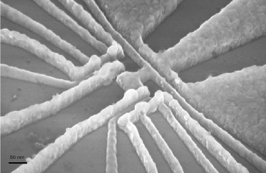
For quantum computers based on spintronics like silicon quantum dot qubits ², patterning with sub-5 nm overlay creates high-density electrodes, sometimes more than ten, with critical dimensions below 10 nm in order to interrogate a 100 nm x 100 nm area containing multiple quantum dots (see figure 1).
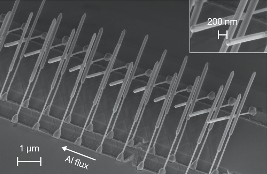
On the march towards topological qubits, nanofabrication is utilized to create the indium antimonide nanowire devices (see figure 2) that demonstrate quantized Majorana conductance ³, a big step towards someday experimentally realizing the topological qubit for the first time.
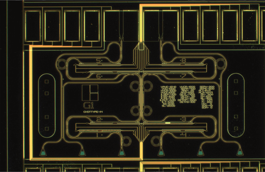
For realizing qubits with nanophotonics (figure 3), Raith lithography systems are used to create the waveguides, grating couplers, and microring resonators with very low line-edge roughness and picometer-level precision ⁴,⁵.
For qubits based on vacancy color centers, electron beam lithography and focused ion beam are used to create nanocavities and solid immersion lenses for controling the optical modes in the vicinity of the color center.
Finally, maskless single ion implantation with Group IV focused ion beams deterministically positions Group IV color centers with nanometer-level accuracy ⁶,⁷.
Our solutions for quantum technology
Nanofabrication is advancing the development of most of the competing qubit technologies. Raith’s state-of-the-art electron beam lithography and focused ion beam nanofabrication instrumentation, and the people behind these technologies, play a critical role in fabricating qubits for quantum computing and in quantum technologies in general. Knowing this, Raith will focus squarely on producing the technologies required to meet the present and future needs of the research community who are working diligently to bring the benefits of quantum mechanics to our world.
Do you have any questions about whether the Raith systems will fulfill your specific research or fabrication need? Get in touch with us now and we will happily evaluate your requirements.
PUBLICATIONS
[1] Gabriel Popkin, Quest for qubits, Science, 354, 1091 – 1093 (2016).
[2] R. Mark Wilson, Silicon-based quantum dots have a path to scalable quantum computing, Physics Today, 71, 17 (2018).
[3] Hao Zhang, Chun-Xiao Liu, Sasa Gazibegovic, Di Xu, John A. Logan, Guanzhong Wang, Nick van Loo, Jouri D. S. Bommer, Michiel W. A. de Moor, Diana Car, Roy L. M. Op het Veld, Petrus J. van Veldhoven, Sebastian Koelling, Marcel A. Verheijen, Mihir Pendharkar, Daniel J. Pennachio, Borzoyeh Shojaei, Joon Sue Lee, Chris J. Palmstrøm, Erik P. A. M. Bakkers, S. Das Sarma and Leo P. Kouwenhoven, Quantized Majorana conductance, Nature, 556, 74–79 (2018).
[4] C. Schuck, X. Guo, L. Fan, X. Ma, Menno Poot and H. X. Tang, Quantum interference in heterogeneous superconducting-photonic circuits on a silicon chip, Nature Communications, 7, 10352 (2016).
[5] Raith application note Menno Poot
[6] Junfeng Wang, Xiaoming Zhang, Yu Zhou, Ke Li, Ziyu Wang, Phani Peddibhotla, Fucai Liu, Sven Bauerdick, Axel Rudzinski, Zheng Liu and Weibo Gao, Scalable Fabrication of Single Silicon Vacancy Defect Arrays in Silicon Carbide Using Focused Ion Beam, ACS Photonics, 4, 1054–1059 (2017).
[7] Yu Zhou, Zhao Mu, Giorgio Adamo, Sven Bauerdick, Axel Rudzinski, Igor Aharonovich and Weibo Gao, Direct writing of single germanium vacancy center arrays in diamond, New Journal of Physics, 20, 125004 (2018)