World of Metrology
Fabricating nanostructures is an art and a science of its own. A key success factor in micro- and nanotechnology consists in monitoring a wafer along its complete process chain. Full process control can only be achieved if the dimensions and position of the fabricated structures are evaluated continuously. In order to optimize and maintain accuracy, reliability, and repeatability of the results, fast and automated generation of metrology data is mandatory for state-of-the-art nanofabrication processes.
The most versatile approach for top-down metrology applies a focused electron beam (e-beam). When the e-beam scans a wafer surface pixel by pixel, the intensity of secondary electrons (SE) is directly correlated to the surface topography. An ultra-fast SE detector (either beside or inside the electron column) collects these secondary electrons. The intensity of SEs at each pixel is converted to a grayscale map of the wafer surface. Additional information, e.g. about the chemical composition of the substrate, can be obtained simultaneously by detecting ‘backscattered electrons’ (BSE) with a dedicated BSE detector.
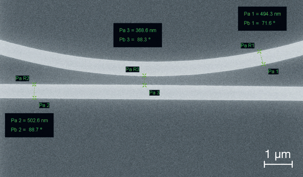
Instead of acquiring a complete image, the e-beam can also be scanned in line mode across a given topography. In this mode, surface information can be obtained much faster compared to full image scans. The data can be further evaluated in xy graphs to measure e.g.
- position,
- dimension,
- distance,
- shape, or
- pitch
of single or multiple structures.
Automation – It’s the difference that makes the difference
Of course performing metrology as described above on individual structures is a straightforward procedure. But what to do if several thousand structures on a wafer must be characterized as fast and precisely as possible?
In this case automation of the metrology process is essential. It typically contains several steps:
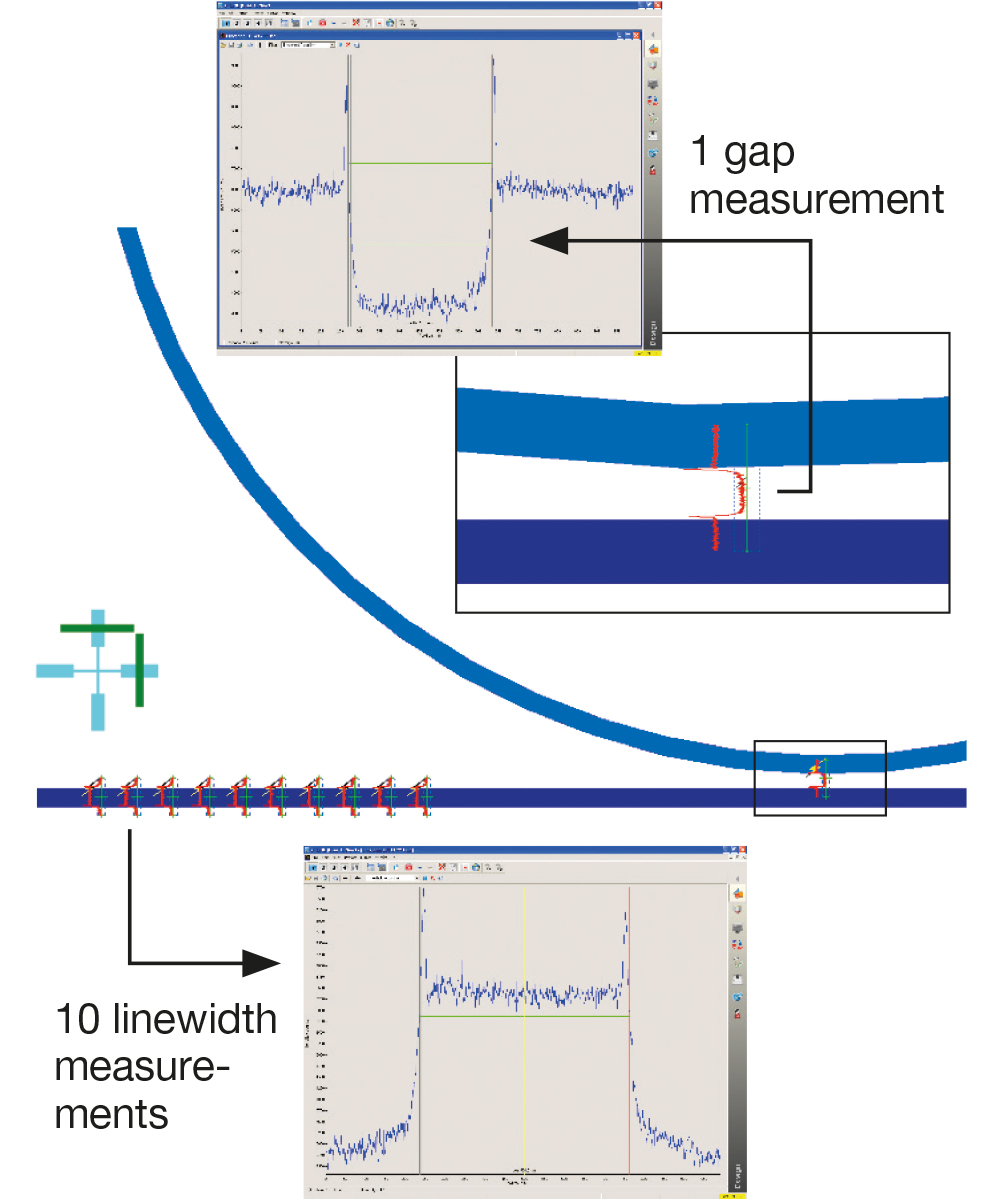
Step 1: Metrology data is generated by addressing the e-beam to the target position of each structure fast and precisely. A line scan is performed at this position and the data obtained are evaluated automatically on the fly. Results such as positioning accuracy or lateral dimension of a structure are available instantaneously.
Step 2: In an offline post-processing step, the metrology data can be exploited in more detail. E.g. to measure the pitch between two structures their position is automatically correlated.
Step 3: The obtained data is post-processed for statistical analysis and further evaluation using additional dedicated software tools.
Limited sample size
First of all, SEMs are most commonly designed for investigation of samples only a few cm in diameter. Professional complete wafer handling typically exceeds the capacity of such instruments. Automated height measurement and sample leveling is mandatory for wafer-scale metrology processes to keep the e-beam in focus on the sample – something that cannot be done with conventional SEMs, even on smaller samples.
Stage accuracy
Second, in every SEM column the range of the beam deflection is limited to ~mm distances. This implies that arbitrary positions on the wafer scale can be addressed only by moving the sample stage of the SEM to the target position. This of course requires accuracy of stage positioning in the range of ~nm, which is typically far beyond the accuracy of conventional SEM stages.
Automation and metrology
Third, conventional SEMs are optimized for acquisition of single images. Even though it is often possible to acquire individual line scans manually, automated scanning of thousands of line scans is not intended for this class of instruments. In addition, quantitative analysis of line scan data is not possible in most cases.
EBL systems - A way out?
Many of the mentioned limitations of conventional SEMs can be overcome by state-of-the-art electron beam lithography (EBL) systems. These instruments are designed for handling and addressing wafers more than 200 mm in diameter. They are equipped with fast and high-precision stages on which wafers can be levelled. However, many of these tools are developed as pure writing systems for nanofabrication, and as a consequence their software typically does not provide extended metrology capabilities.


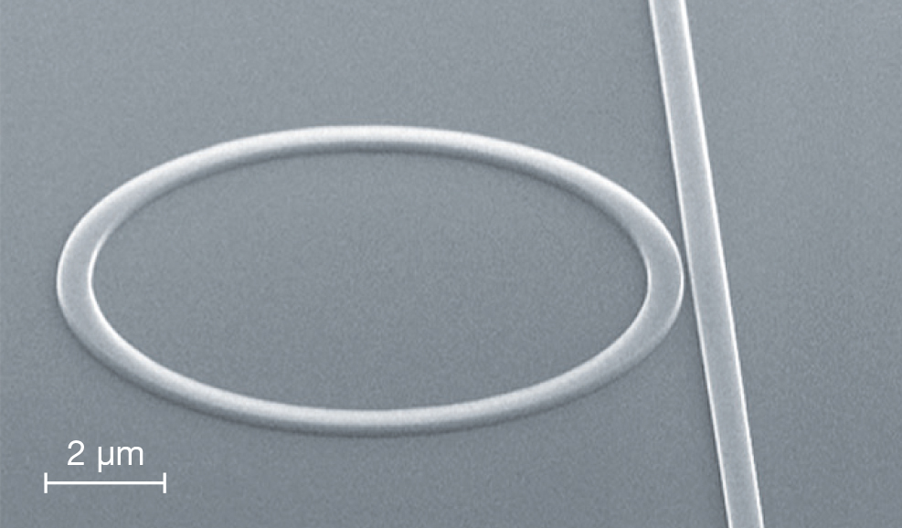
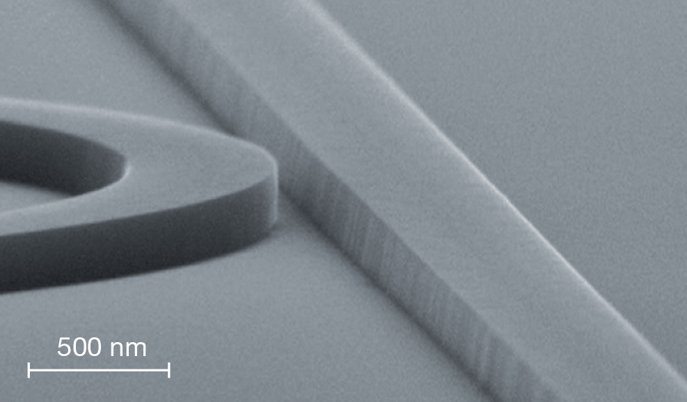
All images: Linjie Zhou, Katsunari Okamoto, and S. J. Ben Yoo, et al., University of California Davis, and James Conway, et al., Stanford Nanofabrication Facility
Bridging the gap
Obviously there is a gap between automated high-resolution metrology and large-area high-volume nanofabrication applications. Several of Raith’s electron beam lithography (EBL) instruments bridge this gap and combine the best of these two worlds: the world of metrology and the world of e-beam lithography.
The best of both worlds – Metrology using Raith EBL Systems
In many of Raith’s EBL systems the e-beam can be addressed to any position on a wafer of up to 150 mm diameter (200 mm wafers can be loaded). All of Raith’s instruments are equipped with a high-precision laser-interferometric stage as default. This allows the operator to address any arbitrary position on a wafer with ~nm accuracy.
The key to success in terms of metrology is then a combination of precise positioning of the sample stage and subsequent deflection of the e-beam.
Finally, the software offers automated acquisition of thousands of line scans without any user interaction. Long-range metrology such as pitch measurement of a grating of several mm length can be performed straight away. Evaluation of the measurement data is performed either on the fly or offline in a post-processing step. Results can be visualized immediately within the software user interface. In addition, data can be exported for further evaluation with third party software.
Multiple tasks - One solution
Many of Raith’s EBL instruments cover multiple tasks in one single instrument. This approach turns the science of nanofabrication into a pleasant and cost-effective art. Get in touch with us to discuss your options.