Proximity effect correction – Getting your design precisely implemented on every sample
The proximity effect in electron beam lithography
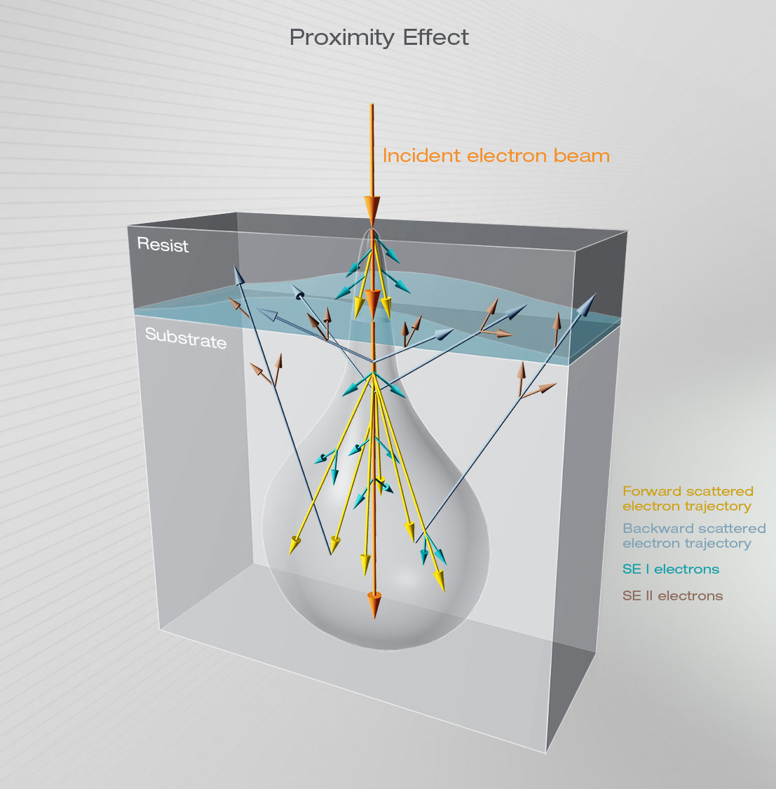
In Gaussian electron beam lithography (EBL) a resist layer on a substrate is typically patterned directly by exposing the sample with a focused electron beam. However, the primary electrons of the beam are scattered in the resist layer (forward scattered electrons, FE) as well as in the substrate material beneath (backscattered electrons, BE). These scattered electrons create secondary electrons (SE1 and SE2) on their way through the resist, which both contribute to the total exposure dose at all substrate regions (see Figure 1). This means that regions adjacent to those initially addressed by the electron beam will receive a higher total electron dose than originally intended. As a consequence, a designed pattern will be implemented imprecisely on a sample with respect to size and shape. In literature, this effect is well known as the proximity effect.
The impact of the proximity effect depends highly on the density and atomic weight of the substrate material as well as on the energy of the primary electron beam. In addition, the design itself has an influence on the pattern fidelity: If both large and small structures are placed close to each other, the variation of the pattern density leads to a variation of the total electron dose at each point of the design.
Mathematically, the actual energy distribution given by the primary and scattered electrons (FE & BE) can be approximated as the weighted sum of several Gaussian distributions, which, in principle constitute the “proximity function.”

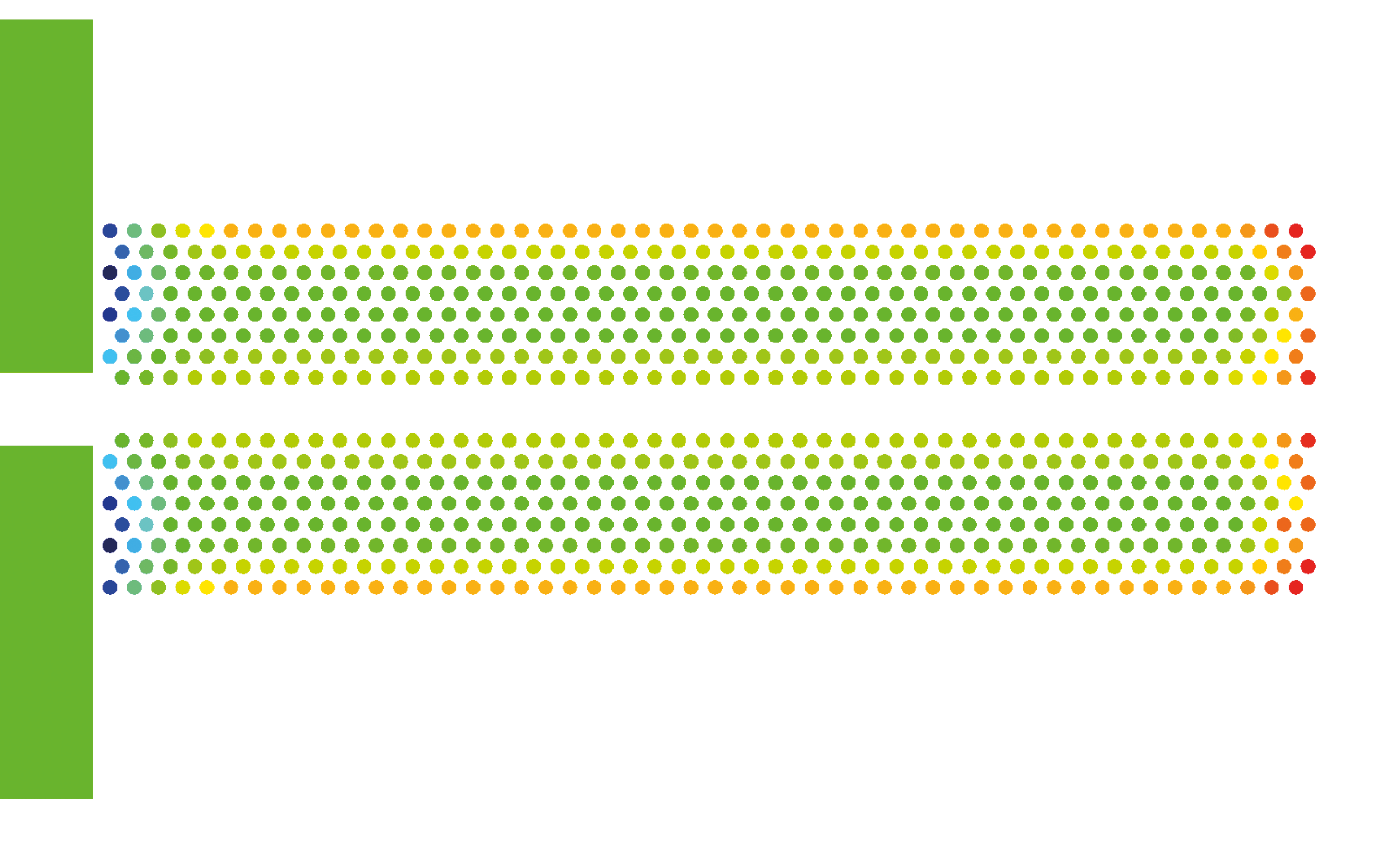
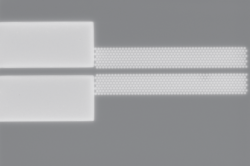
Figure 2: Photonic crystal exposure optimization using NanoPECS proximity effect correction package with the help of proximity corrected dose distribution
Questions?
If you have any questions or need more information, just get in touch!
The proximity effect can be compensated for by adjusting the initial electron dose distribution in the design. This process is called “proximity effect correction” and requires comprehensive and computationally intensive processing. The aim of a proximity effect correction is for every point of the design to receive effectively the same electron dose, resulting in maximum possible pattern fidelity.
To perform a proximity effect correction, it is necessary to
Adjusting the energy distribution for proximity effect correction
-
- determine the parameters of a proximity function for FE and BE
- fracture large structures of a design into smaller pieces
- assign individually corrected dose factors to each piece
Optimize your structure with nanoPECS
Raith’s solution for proximity effect correction is the optional software nanoPECS™. It is integrated into the GDSII module of the NANOSUITE software and simplifies proximity effect correction, even for unexperienced users.
In nanoPECS™, a proximity effect correction is performed in 5 consecutive and mostly automated steps:
- Definition of the proximity function which describes the energy deposition vs. radial distance from the exposed pixel. nanoPECS™ offers the combination of up to 3 Gaussian functions plus 1 exponential function to form the final proximity function.
- Fracturing of the different elements of the design into smaller pieces
- Combining the smaller pieces into manageable partitions
- Computing a proximity effect matrix (PEM) for the corrected dose factors
- Assigning the calculated dose factors to the design

The software consists of 3 major functional parts:
- nanoPECS proximity correction
This is the core function of nanoPECS™. In order to support users as much as possible, a wizard can be activated which guides them through the procedure of parameters setting. Simply start it within the software and select the voltage and material being used, and the software will prompt values that match all relevant parameters. Users preferring not to rely fully on the automated proposals also have the option of editing each parameter manually.
The software finally runs a full proximity effect correction. The resulting modified design can be exposed right away.
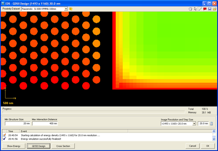

Figure 3: Energy density simulation of a photonic crystal exposure optimization using nanoPECS: the GDSII dose distribution and the simulation of the deposited energy in the software.
2. nanoPECS proximity parameter database
In this part of the software, sets of parameters for different situations can be created, stored and modified. Proximity parameters can be edited in three ways:
- Manually. In this case the parameters have been determined from prior experiments or are based on values that can be found in literature.
- Data interpolation. After selection of the approriate beam energy, substrate material, and resist, the software calculates a set of proximity effect correction parameters which can be stored in the database
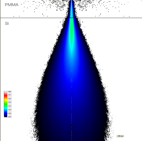
- Monte Carlo simulation. In this simulation the trajectories of e.g. 1 million electrons are calculated and the scattering parameters are derived by fitting the proximity function(s) to the simulated data. Up to 4 different proximity functions can be stored in the database. The simulation works for every type of material as it is based on its own material database. Data of new material can be added easily by the user.
3. Energy density simulation
After a design is successfully corrected, the expected energy distribution after a simulated exposure can be displayed in a 2-dimensional map. In addition, a 3-dimensional animation allows the user to estimate the expected quality of the proximity effect correction at any place in the design. The dose distribution can be optimized even before a real exposure is run.

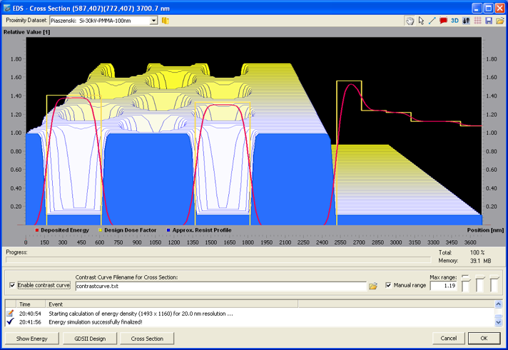
Figure 5: Energy density simulation as a 3D Plot of a Cross Section
nanoPECS™ is an extremely useful tool which can be fully integrated into the Raith NANOSUITE software. nanoPECS™ offers an easy and affordable solution to overcome the proximity effect in EBL. It is possible to upgrade your software with nanoPECS anytime. Get in touch with us to discuss the options!