VELION

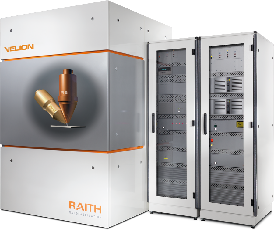
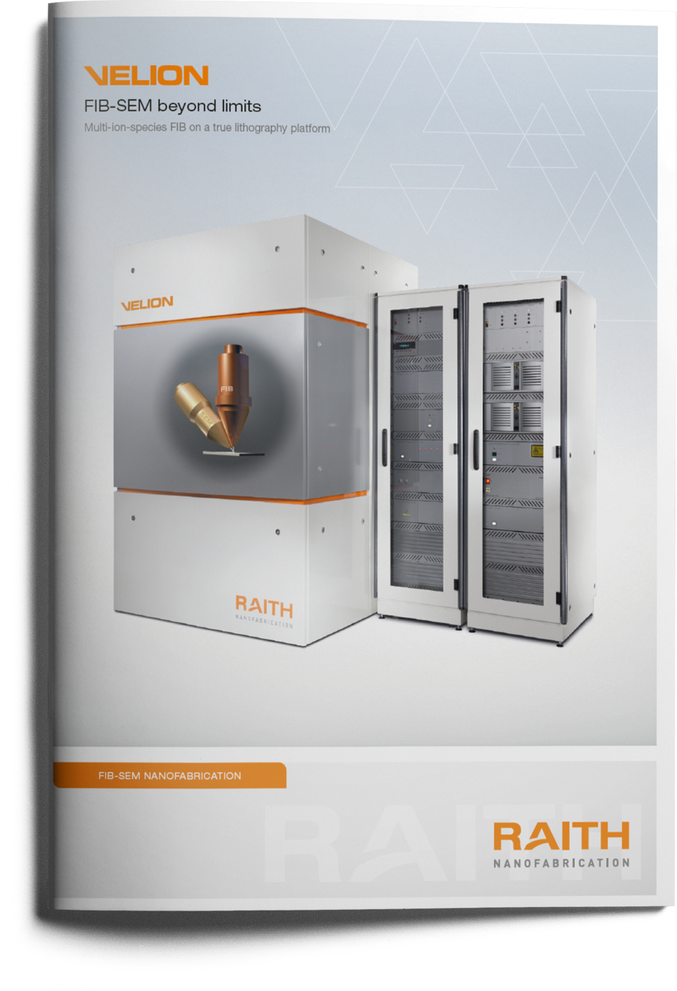
Multi ion species FIB‑SEM

Introduction

VELION represents a groundbreaking FIB-SEM concept tailored for nanoscale science and engineering applications. FIB nanofabrication excels in creating intricate three-dimensional and high-resolution nanostructures like plasmonic devices, nano-fluidics, localized ion implantation and sample functionalization.

Rising to the challenge of meeting the rigorous demands of nanofabrication with its FIB on a true lithography platform, configurable multi-species FIB technology, cutting-edge FIB performance, and ion microscopy capabilities for generating the highest resolution 3D images.

Key features

  • Unique multi-ion-species FIB technology (IonSelect)
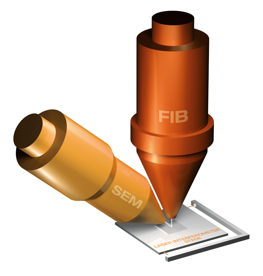
  • Vertically mounted FIB column and horizontal 4-inch laser interferometer stage
  • Large-area FIB patterning capabilities on a true lithography platform
  • Automated, stable nanofabrication over several days
  • Ga-free TEM sample preparation
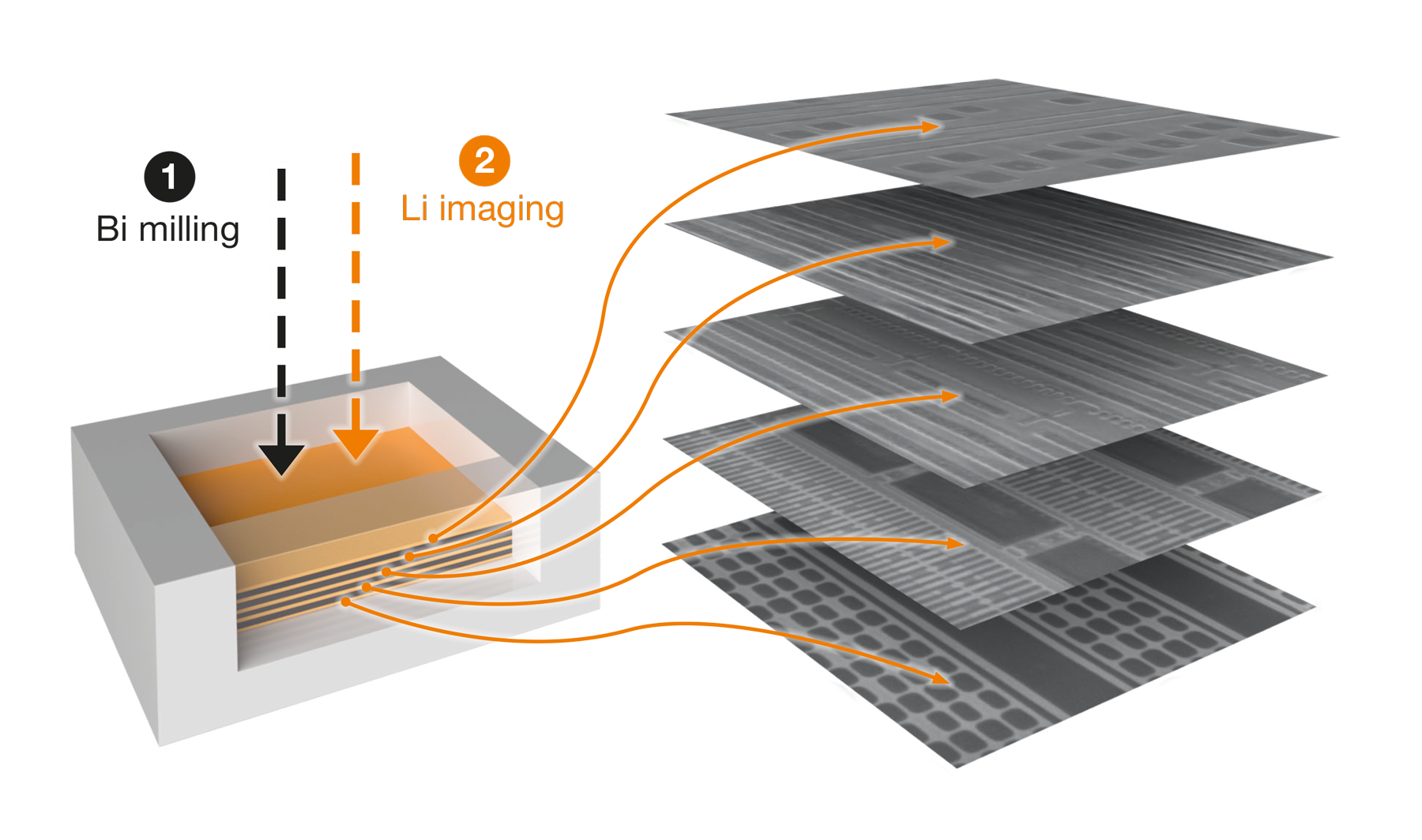
  • Ion microscopy and imaging with light ions
  • Easy, fast and reliable ion imaging, 3D sample reconstruction without stage tilt
  • Sample analysis & in-situ process monitoring enabled by tailored SEM column
Benefits

It’s all about FIB in perfection

Multi ion species FIB technology

With the ability to select from a variety of ion species, VELION empowers precise adjustment of nanostructures offering unlimited process possibilities.

Cutting edge FIB performance

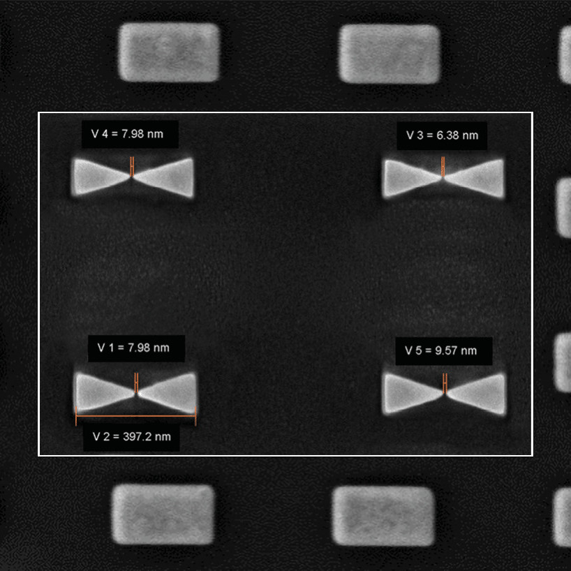
Achieve sub 10 nm FIB resolution with unparalleled precision. Dynamic beam corrections deliver excellent write field calibration, ensuring precision at every step.

Unmatched large area FIB patterning

VELION unlocks unique FIB patterning capabilities on a lithography platform, offering unparalleled capabilities. Features include large-area FIB imaging, seamless write stitching, continuous writing modes for flawless nanopatterning, and full 4-inch wafer processing for rapid prototyping and small-batch production.

Stable nanofabrication over extended periods

VELION offers stable and accurate nanofabrication over several days. Along with reproducible sample positioning, CAD overlay and a high degree of automation, unattended high-end nanoengineering becomes possible.

Fast

Scan

Software

Accessible professional lithography: Ergonomic interface for all users

Designed for automated nanoengineering
The proprietary Digital RAITH Nanosuite control software, with its various modules, is the most comprehensive and fully integrated nanolithography software available.

Single software platform

System operators can efficiently control all system functionalities and exploit its capabilities from a unified software platform.

Control with digital column

Fully digital controlled column including parameter sets save and reload.

Flexible mark recognition and automation

Extremely flexible mark recognition, automation and design handling.

Python scripting

Interface with Python scripting for extended automation and customizing.

GUI workstation

Windows-based GUI workstation and a second software license for offline data preparation.

Mill & image

A dedicated GUI streamlines Mill operations, while an optimized image workflow supports tomography and 3D sample reconstruction.

GDSII CAD-editor

Complete patterning capabilities with GDSII CAD-editor, including advanced beam control and convenient parameter handling using recipes.

Multi-user environment

User authentication is required for logging in, and different user levels allow access to specific sensitive system parameters.

Patterning on image

For rapid prototyping, process development and optimization.

Process monitoring

Real-time process control and endpoint detection with movie functionality.

TEM lamella preparation workflow

For high quality Gallium free TEM sample preparation.
100 person-years of software programming

Technical data

Access to multiple ion species from a single source
3
Lithography platform
Full 4″ wafer processing
Field stitching and overlay accuracy
< 50 nm
(|mean| +3·sigma)
Feature size
< 10 nm direct milling
Are you interested in more details and insights?
VELION Product Brochure (.pdf)
Application note: Device trimming of photonic integrated circuits through efficient combination of EBL and FIB (.pdf)
An advanced fabrication techniques combing EBL and FIB can perfect integrated photonic circuits for cutting-edge applications. This application note explores precise post-fabrication tuning using RAITH's electron beam lithography and focused ion beam patterning. Learn how to correct fabrication imperfections with sub-picometer accuracy for optimized photonic devices, revolutionizing data interconnects, sensors, AI accelerators, and quantum technologies.
Whitepaper: nanoFIB column (.pdf)
Lean how to utilize RAITH’s nanoFIB column with its long-term stable ion beam current at lowest position drift and lowest beam tails to advance FIB nanofabrication to the level of a lithography system. The Whitepaper describes the state-of-the-art focused ion beam column technology and its key strengths to achieve cutting-edge application results.
Whitepaper: FIB-SEM nanofabrication (.pdf)
Learn how to benefit from resistless FIB nanofabrication and how to get access to a wide range of applications which are beyond the reach of common FIB-SEM and EBL instruments. The Whitepaper highlights typical applications that can be addressed with VELION, such as 3D nanostructures at once over mm length, FIB hard masking of large area patterns and many more.
Whitepaper: Multiple ion species for FIB with IonSelect (.pdf)
Learn how the unique IONselect technology gives you the chance to utilize light or heavy and swift or slow ions from universal ion sources. Immediate switching between different ions paves the ways for new lithography process pathways. The Whitepaper describes the innovative source technology of Raith’s nanoFIB column with IONselect and its availability of various ions for FIB nanofabrication.
Whitepaper: GaBiLi – the next generation FIB source for 2D and 3D ion imaging (.pdf)
Find out how to get high-resolution 2D and 3D images of your sample, utilizing light and heavy ions from the same source for ion microscopy. The Whitepaper describes the functionality and benefits of the multiple-ion-species FIB column in combination with a mature lithography platform to easily achieve precise 3D sample reconstruction.
Application Note: Advanced gallium-free TEM lamella preparation using VELION FIB-SEM (.pdf)
High quality TEM lamellae are crucial for high-resolution TEM characterization. Using a vertical FIB column with multiple ion species for TEM sample prep yields many advantages. ThIs application note highlights how to use VELION’s unique features to advance the quality of TEM investigations and to optimize TEM lamella prep for a wider range of materials.
Application Note: Ion beam lithography for Fresnel zone plate fabrication in gold on membranes (.pdf)
Fresnel zone plates are widely used as diffractive-based focusing elements in X-ray microscopy, achieving resolutions down to 25 nm. While they are typically prepared by EBL, this application note shows how the fabrication of zone plates by a dedicated FIB nanofabrication system (RAITH ionLINE) is able to significantly reduce the fabrication steps while still deliver the necessary high resolution.
Application Note: Sketch & Peel (.pdf)
A standard adhesive tape can help overcome the relatively slow patterning speed of direct FIB milling. The Application Note explains the new sketch & peel approach in detail and also investigates the change in outcome when using different ion species. Learn how simple adhesive tape can help you increase your throughput up to several orders of magnitude compared to usual FIB milling.
Application pattern

Versatile application space

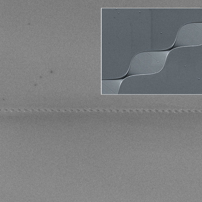
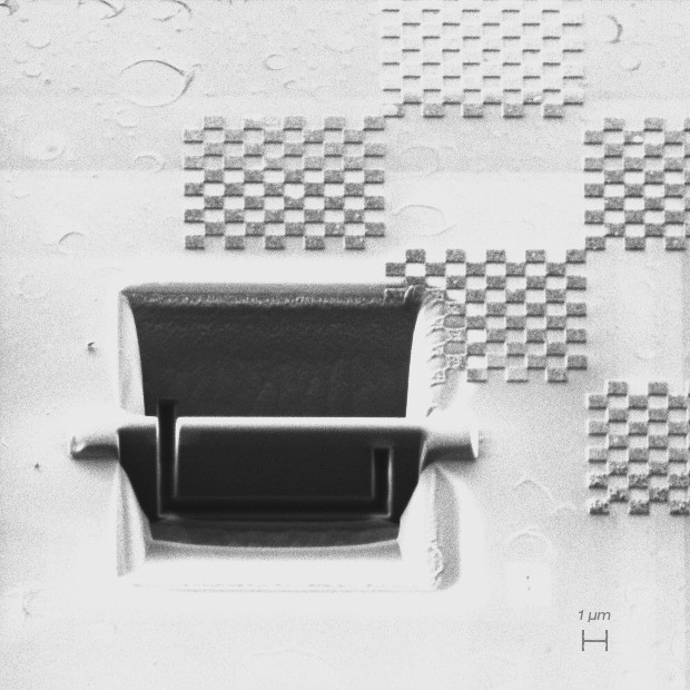
3D stitching and FIB milling enables a 1 mm long microfluidic mixer channel, Argonne National Laboratory
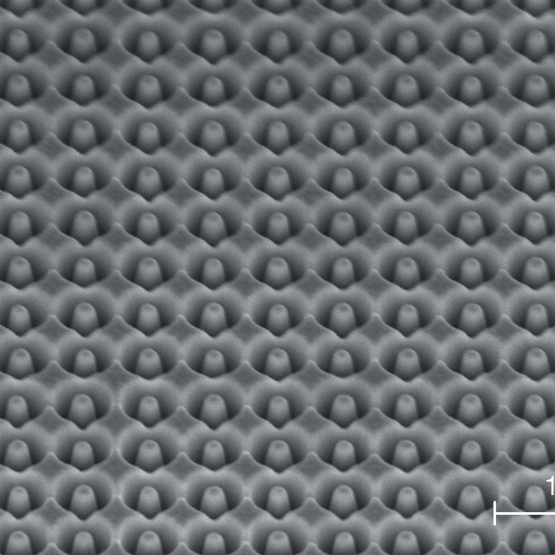
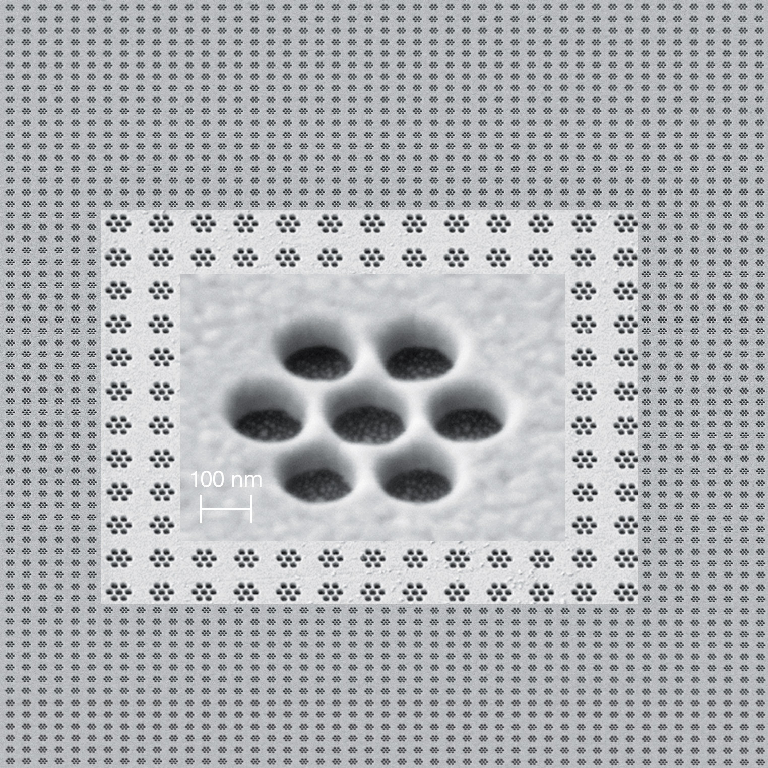
Large plasmonic array of small features created by direct FIB milling in gold, University of Stuttgart
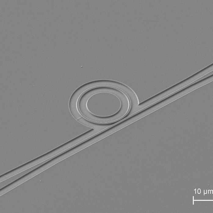
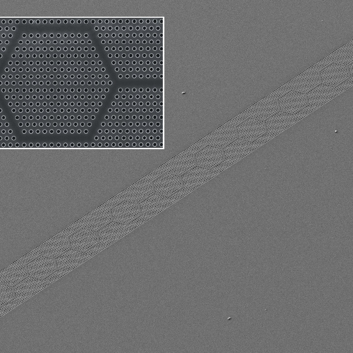
Photonic device of waveguide and coupler, Peking University
Meta surfaces
Long-term processing for large and complex shapes such as a 3D nano absorber structure, Zhejiang University
TEM-sample preparation (Gallium-free)
Cross-section area of CMOS device
(Massachusetts Institute of Technology)
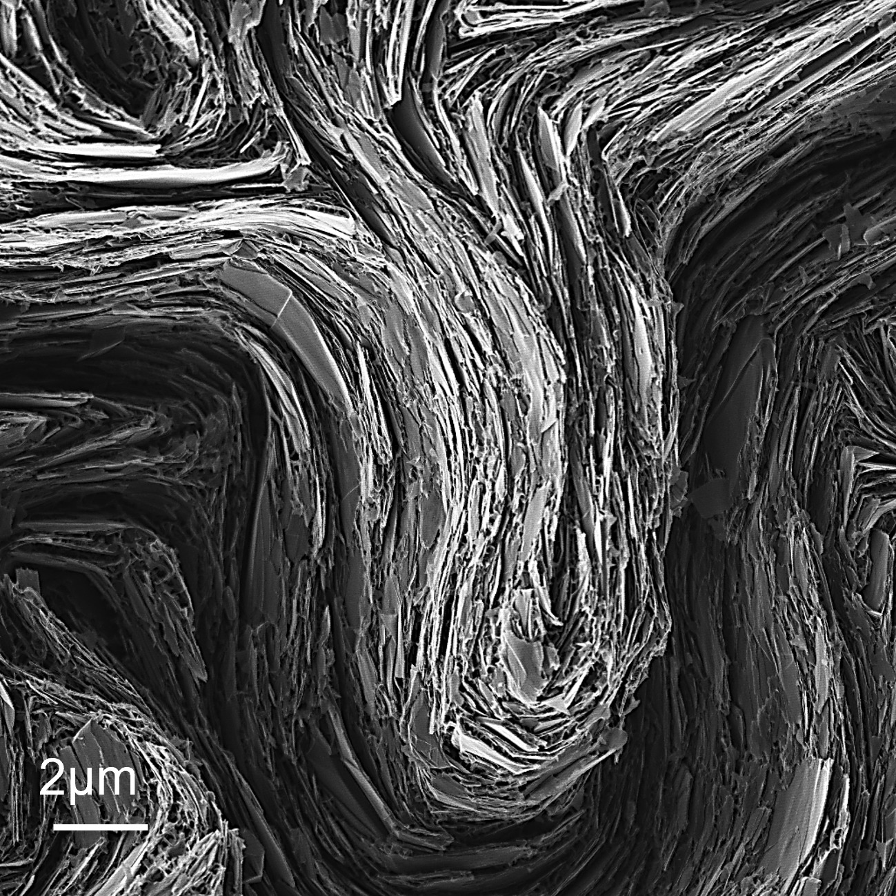
Lithium ion images of diatoms
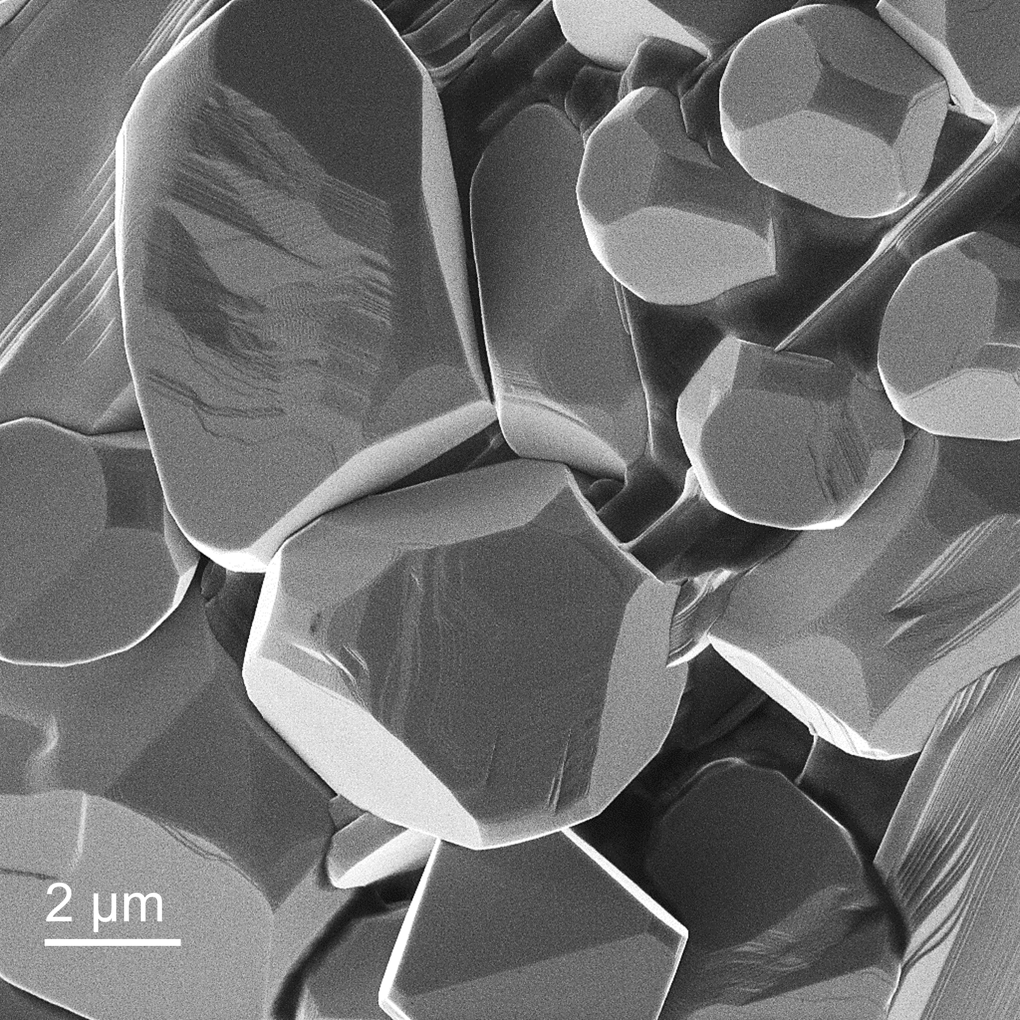
Large area FIB imaging and mosaic stitching
Solutions

RAITH offers integrated solutions that increase performance and create market opportunities. In any production environment.

References
It should be no surprise that we are not able to share project details here. Suffice to say that we’re proud of the work we did with some well-known global tech leaders and leading scientific institutions.
RAITH VELION used at University of Muenster, Germany, marked on a grey map.

VELION at Universität Münster, Prof. Dr. Wolfram Pernice

“We have already been using a RAITH EBPG and an ELPHY on a FIB-SEM microscope for years and were always satisfied with the performance and ease of use of the systems. With VELION, Raith now offers […]

RAITH VELION used at University of California Santa Barbara, marked on a grey map.

VELION at the University of California, Santa Barbara, Dr. Dan Read

I have been working with RAITH and their products for over 20 years at four different research-intensive universities in both the US and Europe. I have always enjoyed my interactions with RAITH […]

To find out which configuration best suits your needs, get in touch with us.
I want to contact a RAITH-Expert
Headline
This is a basic text element.
Headline
This is a basic text element.