Did you know about RAITH’s SEM Instrument Technologies?
RAITH has been a leading expert in nanofabrication, and especially electron beam lithography, for over 35 years. But did you know that Raith instruments also enable automated large–area SEM image acquisition, automated CD–SEM metrology, and linewidth and placement measurements?

Large-Area SEM Imaging and SEM Metrology
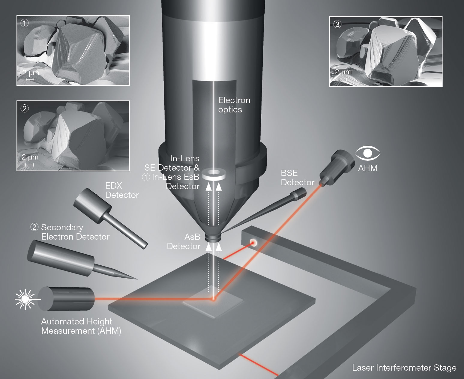
Nanofabrication has become ever more sophisticated over the years, and our instruments have kept pace. While nanofabrication has certainly remained our focus, other less well-known features have either long been on board already, or were added along the way. Today RAITH instruments also support SEM applications that require stability, stage precision, and automation. All RAITH’s turnkey systems provide a variety of nanometrology options and automated routines for qualitative and quantitative process control, allowing them to be used in a “CD-SEM-like” manner. However, RAITH’s CHIPSCANNER produces the most accurate large-area, high-resolution images directly acquired by an SEM instrument, allowing accurate stacking of 2D images for 3D modeling. In addition to the Laser Interferometer Stage and automated height sensing, a range of detectors is available as one of the critical components for accurately stitching SEM images over large areas.
Watch the video below, visit our technology site, or download the brochure to find out all the details about RAITH’s SEM Instrument Technologies.

