Key features
Highest-efficiency surface-sensitive imaging with material contrast even at low kV
Distortion-free, high-resolution, high-efficiency imaging
Detection of surface-sample information only
Simultaneous data acquisition for surface and compositional information
Excellent material contrast even at lower kV
Stable, crisp contrast for long-term image acquisition
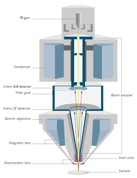
Electron optics design – the key to low kV performance
The Gemini objective lens design combines electrostatic and magnetic fields to maximize optical performance, while reducing field influences at the sample to a minimum. This enables excellent imaging, even on challenging samples such as magnetic materials. Inlens—the Gemini detection concept—ensures efficient signal detection by detecting secondary (SE) and backscattered (BSE) electrons in parallel. Inlens detectors are arranged on the optical axis, which reduces the need for realignment and thus minimizes time-to-image. Gemini beam booster technology guarantees small probe sizes and high signal-to-noise ratios, right down to very low accelerating voltages. It also minimizes system sensitivity to external stray fields by keeping the beam at high voltage throughout the column until its final deceleration.
By combining Inlens EsB- (Energy selective Backscattered), SE- (Secondary Electron), or aBSD- (annular Backscattered Detector) detectors, the system delivers information about the material, topography, or crystallinity of your sample. The primary electron beam generates secondary electrons (SEs) and backscattered electrons (BSEs). The SEs escape directly from the topmost nanometers of the sample with energy of less than 50 eV and represent the topography of the surface. As a result of the unique beam booster concept, these SEs are accelerated back into the column and the Gemini objective lens directs them to the annular Inlens SE detector.
BSEs are generated below the surface and provide highly specific information about the material composition of your sample. BSEs appear conically at a ~15-degree angle to the primary electron beam. They are attracted by the beam booster of the Gemini column and directed into the column. Because of the different energies of SEs and BSEs, they follow different trajectories within the beam booster. Most of the BSEs can pass the Inlens SE detector and are collected by the EsB detector. Additionally, the Inlens EsB detector enables an energy selection of the BSEs. If the takeoff angle is greater than ~15 degrees, the BSEs cannot make their way into the column, but can be detected by an AsB (Angular selective Backscatter) detector that is integrated into the objective lens, precisely fitted into a pole piece cap below the objective lens.
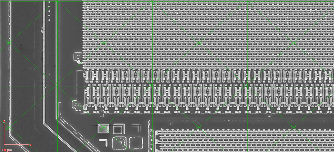
Relevant sample information, whether of topographical or compositional nature, can be accquired over very large surface areas in a fully automated fashion. ProImage technology does all this with highest efficiency and maximum sample information, due to smart detectors and excellent low kV capabilities. Calibrated write fields can be stitched together to provide a mosaic image view of the entire sample from nm to cm scale.


