Key features
Meeting the toughest nanofabrication demands for challenging design geometries
Highest pattern fidelity
Reduced LER
Throughput enhancement
Shapes for lean exposure data handling and optimum results
Fracturing
As a long existing standard, the conventional fracturing of CAD design files for electron beam lithography exposures has been developed and optimized for perpendicularly arranged “Manhattan style” designs. However, given the increasing relevance of highest pattern fidelity with regard to optimum nanodevice performance, this standard method has significant limitations for other pattern design element geometries such as circles, ellipses, rectangles arranged under an angle, etc. RAITH’s revolutionary PerfectShapes technology is based on a design-specific fracturing algorithm and patterning strategy that best approximates the geometrical outline of the individual design element (“shape”).
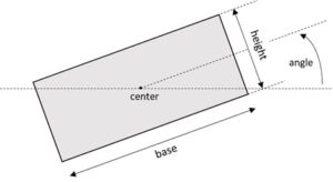
A shape, in the definition of the smallest geometrical design element that is NOT fractured any further, is mathematically defined by various parameters, e.g., origin, offset, center, radius, angle, long axis, short axis, or other, depending on the specific shape of the geometry of the related design element. For the exposure, a specific shape filling mode can be selected to enable the contour of the shape to be perfectly aligned to the geometry of the design element, regardless of its position or orientation in the overall design. Hence, fracturing and beam shot placement are significantly optimized with regard to pattern fidelity, line edge roughness, and amount of data to be processed.
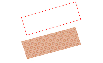
Data volume and data processing:
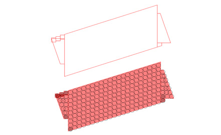
The number of fractured elements can be significantly reduced due to the new shape-based fracturing algorithm. Depending on the design and number of elements, PerfectShapes helps to reduce data volume, resulting in far less process overhead time, but simultaneously increases pattern fidelity and line edge roughness.

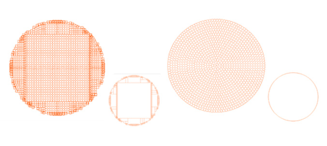
Shape types and derivatives
Circles, ellipses, and cubes (rectangles) are among the most challenging design element types. With PerfectShape, there is no need to fracture these into many small trapezoids, which are the sole shape types available in the conventional process. Given that all these geometrical design elements representing a shape are based on mathematical definitions with various parameters such as offset, center coordinate, inner/outer radius, or start/end angle, many sub-shapes or shape derivatives can be designed.
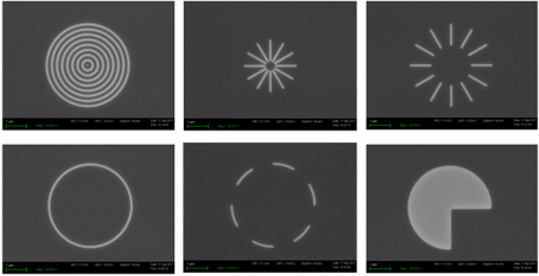
Use case
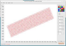
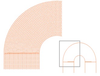
PerfectShapes enables not only complex structures such as those shown above to be created simply by using a single shape derivative, but also an arc, a ring, or a combination of both as a derivative shape of the “circle” shape type. Both of the latter shape derivatives feature prominently in state-of-the-art photonic devicesand certainly have practical relevance.
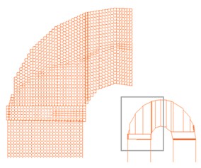
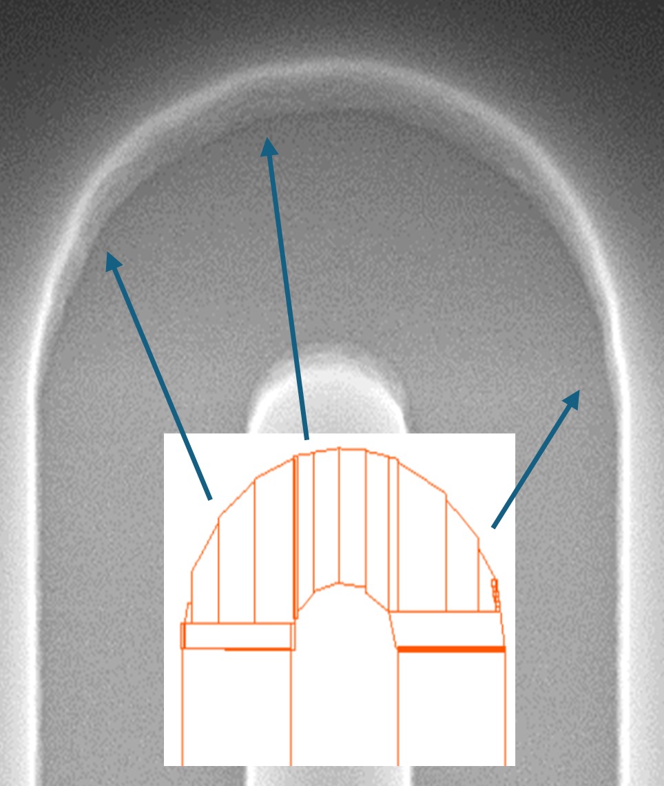
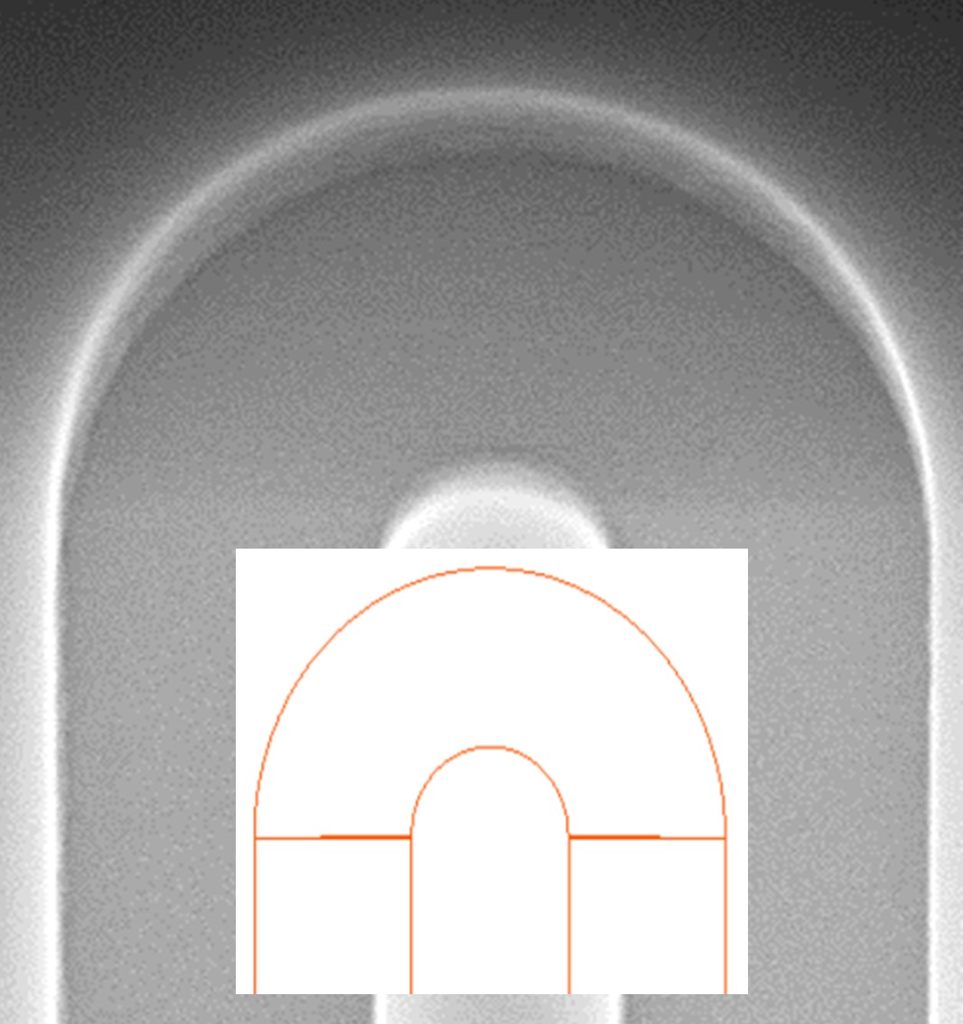
Circles in photonic crystals can be exposed as perfectly round forms using the circle shape with smooth circular shape filling mode. Using the “ring arc” circle shape derivative, a 180-degree waveguide bend exhibits far lower line edge roughness, as can clearly be seen in a comparison of classical fracturing and PerfectShapes technology.
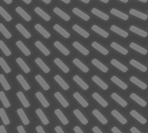
Metalenses, consisting of hundreds of millions of unique individually arranged “nanofins,” are extremely challenging with respect to pattern fidelity and process time overhead, mainly due to the data handling architecture and related computational power required. PerfectShapes technology allows for lean data preparation without the need to create corresponding flat GDSII design data files that may sometimes explode to several hundred GB or even TB. Efficient algorithms enable fast exposures to be performed with minimum overhead and optimum pattern fidelity, as can be seen in a zoom of a metalens shown below. Each nanofin is exposed in the same way, with beam shots aligned to the contour of the rectangle, regardless of its orientation (angle).
