Introduction
Pattern generation is at the core of advanced nanofabrication writing techniques. Achieving resolutions and writing accuracies down to 10 nm or less requires intelligent layout management and high-precision control of both beam and stage movements.
Modern pattern generators provide efficient writing capabilities. They support a wide variety of shapes and flexible, intelligent fill strategies for exposure.
Algorithmic patterning enables the integration of user-defined code for custom shapes and layout formats, providing tailored solutions for new and complex applications.
Accurate stitching supported by laser interferometer stages and stitch-free nanopatterning solutions are essential for maintaining precision and seamless fabrication across write field boundaries for elongated structures. High throughput is critical to support the patterning of full wafers or even larger substrates, ensuring efficiency in large-scale fabrication.
RAITH leads the industry with state-of-the-art direct patterning solutions, offering unparalleled precision and control for seamless fabrication processes.
RAITH customers benefit from extensive expertise and dedicated support, ensuring proper selection and optimal performance of seamless patterning solutions.
RAITH’s track record of success and innovation in seamless patterning speaks for itself, making it the trusted choice for achieving unique and precise fabrication results.
Benefits
Unlocking possibilities
RAITH technologies make even the most challenging designs possible, offering advanced solutions and precise tools for fast design development.
Enhancing final device quality
Various stitch-free methods available for different RAITH tools ensure that your final device quality will not be compromised and will be delivered as it was supposed.
From m² to nm
Achieve sub-micron precision even on 1-meter substrates for flat TV panels with RAITH tools. Our stitch-free technology ensures quality patterning from square meters to nanometers.
Patterning solutions for seamless designs
Elements
When small things needs to be big
Applications for patterning
0 nm
Stitching error
Complete stitch-free strategies: PathControl technology allows entirely stitch-free exposures
1400 x 1400
Millimeters
Unparalleled speed allows submicron patterning over huge substrates up to 2 square meters
1.000.000.000
Elements
A metalens may contain even more elements, all of them need to be positioned with nanometer precision

Waveguides
Stitch-free exposure of photonic circuits with PathControl technology

Photonic crystal
Stitch-free photonic crystal waveguide exposed by periodic patterning
Metalenses
Exposure of large photonic designs without data transfer overhead by algorithmic patterning

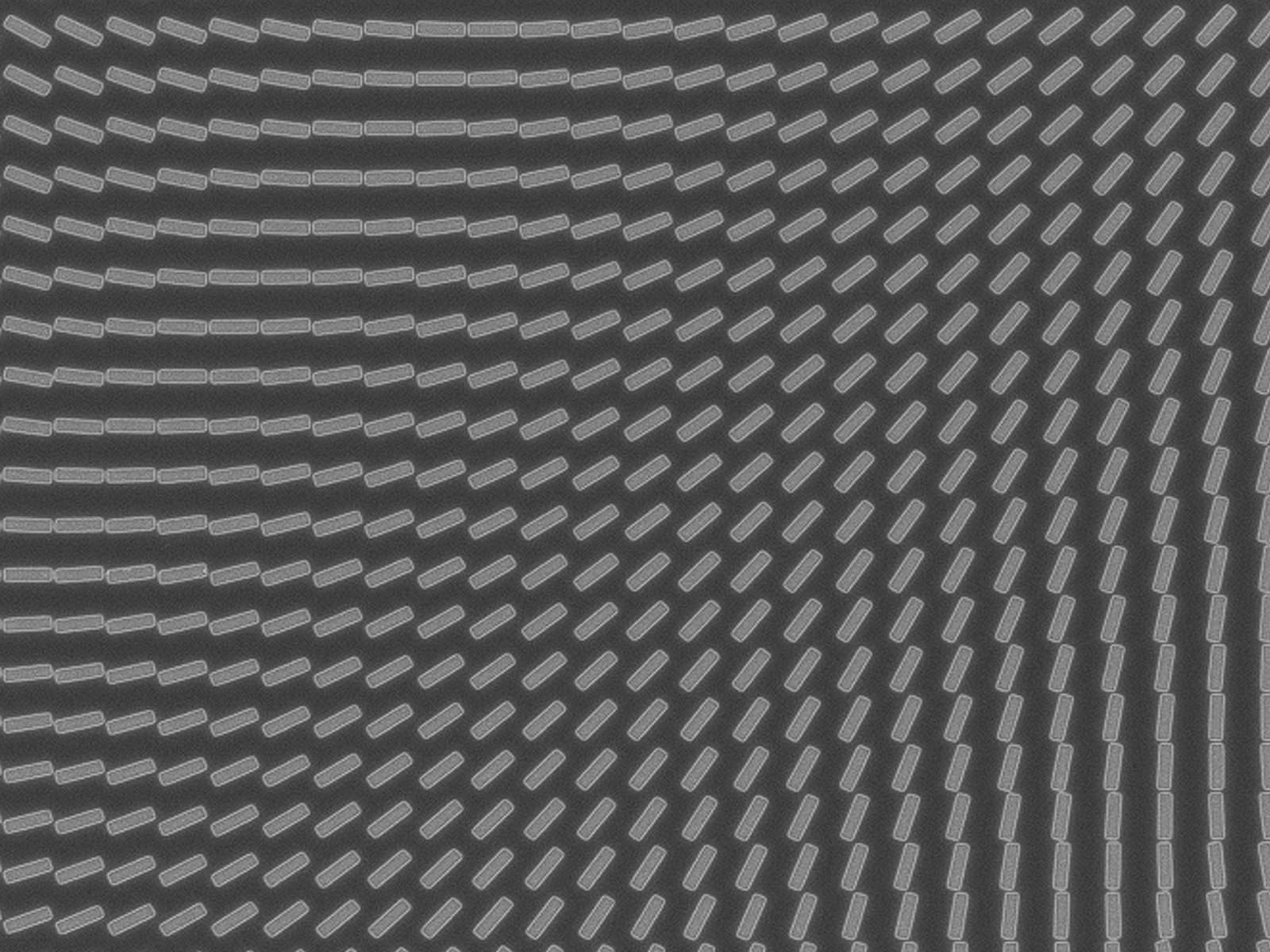
DFB gratings
Pitch control with sub-nm resolution

Complex shapes
User-defined shapes enabled by algorithmic patterning

User-defined data formats
Streamlined pattern transfer with user-fined design data processing by algorithmic patterning