Introduction
Unlock incredible lithography potential with our Mix and Match solutions. We seamlessly blend laser direct writing, ion beam, and electron beam technologies. Our tools empower users to explore new horizons in nanostructuring, enabling precise patterning with unmatched alignment accuracy and flexibility.
Blending electron, ion, and laser lithography
Process development support
Complex patterning across multiple layers
Benefits
Shortest time to results
RAITH’s Mix and Match approach accelerates time-to-result by seamlessly integrating diverse lithography techniques, optimizing workflow efficiency, and empowering rapid prototyping and production processes for faster outcomes.
Throughput
Various Mix and Match strategies enhance throughput by applying different lithography methods to different layers based on accuracy and resolution requirements versus time trade-offs thus maximizing efficiency and accelerating fabrication processes for improved productivity and results.
Unique capabilities
Combining diverse lithography technologies with unparalleled precision enables the creation of unique patterns and devices, unlocking new possibilities for innovation in Academia and fabrication in Industry.
Mixing different lithography methods with ease
Process
One Mix and Match solution to rule them all
01
Design layers for different techniques are automatically transformed into corresponding tools input formats.
02
Coordinate systems of all RAITH tools are easily transformed from one platform to another.
03
Alignment can be done on global wafer scale or die-by-die.
04
Inspection steps with RAITH dedicated process control tools can be automatically set up for each exposure step.
Features
When one technology is not enough RAITH bridges two
Applications Mix and Match
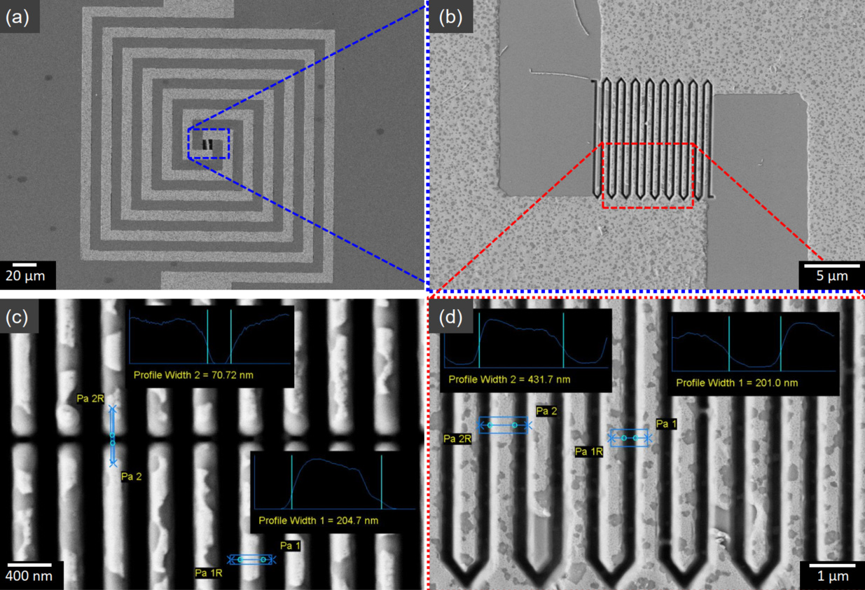
High Electron Mobility Transistor
A High Electron Mobility Transistor (HEMT) with a T-gate enhances performance by reducing gate resistance and capacitance, thereby improving high-frequency response in advanced communication systems and radar technology. The T-gate is added in an EBL mix and match process step between source and drain, which are generated by optical lithography.
Terahertz antennas
Terahertz antennas are made by combining UV photolithography, EBL and FIB techniques: First nanoelectrodes are patterned using EBL. Then a THz antenna fabricated in the second step using photolithography. In the last fabrication step, the shape of nanoelectrodes was modified by FIB.
Waveguide modification
Mix and match process using EBL to populate existing waveguides with additional photonic crystals.