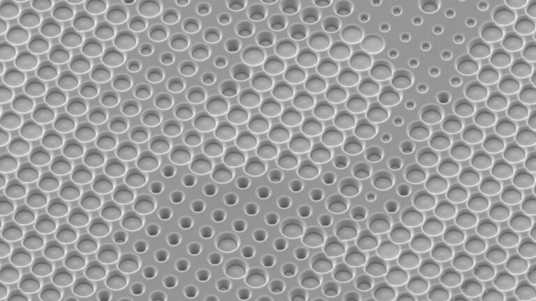
Research / Rapid Prototyping

Pushing boundaries: Advancing science and devices

Introduction

Research has proven to yield invaluable improvements in the understanding of scientific fundamentals, resulting in renowned publications and even Nobel Prize awards. Feasibility studies and rapid device prototyping naturally follow from this knowledge gain, accelerating the design process of future products. This knowledge is closely monitored and utilized in optical telecommunication, consumer electronics, life sciences, nanotechnology research, and beyond.

Advancing the frontiers of mankind

Expert nano- and micro-community

Unlocking scientific potentials

Maskless nanofabrication enables
rapid and efficient prototyping

Your applications

In the dynamic landscape of scientific exploration, predicting tomorrow’s needs can be challenging. That’s why we offer flexible system configurations and field upgradability, combined with ultimate versatility and multifunctionality across our entire product range. Suitable for R&D and enabling a broad range of fundamental research, our solutions support numerous applications across all scientific disciplines. They empower you to effortlessly produce multiple scientific papers or swiftly develop prototypes.
Research / rapid prototyping in topolocigal pyhsics.
Topological physics
Artificial intelligence
Are you interested in more details and insights?
Application Note: Automated nanocontacting of randomly distributes 1D and 2D materials (.pdf)
Transforming randomly distributed 1D and 2D material into functional devices with the help of SEM mapping and innovative offline data preparation for direct-write lithography.
Application Note: Sub-nm pitch control of stitching-error-free millimeter-long periodic structures (.pdf)
Modulated Beam Moving Stage (MBMS) technology enables the fabrication of periodic structures like distributed feedback (DFB) gratings and photonic crystal waveguides.
Application Note: Continuous electron beam lithography writing mode for optical waveguide nanofabrication (.pdf)
Fixed Beam Moving Stage (FBMS) exposure technology can be used to fabricate perfect stitching-error-free arrayed couplings and tapered waveguides up to several millimeters in length.
Application Note: Photonic circuits for on-chip quantum optics (.pdf)
EBPG is utilized to develop an on-chip approach with integrated optics for quantum computing, facilitating secure communication and the simulation of complex systems.
Application Note: Metalens Fabrication (.pdf)
Algorithmic pattern preparation for metalens fabrication achieves high throughput, bypassing design layout conversion, ensuring precision.
Our solutions

RAITH offers integrated solutions that increase performance and create market opportunities. In any production environment.

Enable Research and Rapid Prototyping

Our process

Precision: Our passion in workflow and nano fabrication

01

Needs analysis

Understanding your requirements is paramount. Our team conducts a thorough analysis, delving deep into your objectives, challenges, and expectations to ensure a tailored solution that seamlessly integrates with your workflow.
02

Expert consultation

With our experts by your side, we navigate through complexities together. We offer expert guidance and insights, collaborating closely to develop strategies that align perfectly with your goals and objectives.
03

Feasibility study

We conduct rigorous feasibility studies, meticulously evaluating options and assessing potential outcomes. Our goal is to deliver results that not only meet but exceed expectations, ensuring the seamless integration of solutions that drive your success.
04

RAITH membership

Unlock the full potential of seamless integration by becoming a RAITH member. Gain access to exclusive resources, support, and updates, empowering you to stay ahead of the curve and maximize the value of your integrated solutions.
References
We are supporting a variety of customers ranging from R&D labs in governmental environment or global tech companies to all kind of even Nobel-prize winning academic research facilities.

EBPG at University of California, San Diego, Maribel Montero

The main user and specialist of the EBPG installed at UCSD is Maribel Montero. She provides insights into her daily work with the system and explains why she is a satisfied RAITH […]

RAITH IONLINE and E-LINE Plus used at university of stuttgart in germany, marked on a grey map.

ionLINE Plus and eLINE Plus at the University of Stuttgart, Prof. Dr. Harald Gießen

“Our institute is focused on research in the field of ultrafast nanooptics. High quality and reproducible EBL is essential for the fabrication of nanopatterns for plasmonic structures and […]

To find out which configuration best suits your needs, get in touch with us.
I want to contact a RAITH-Expert
Headline
This is a basic text element.
Headline
This is a basic text element.