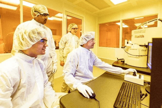
“At the University of Queensland, we recently bought two Raith EBL systems: the eLINE Plus, which was commissioned in 2017, and the EBPG, which arrived in 2018. This has revolutionised […]
“NanoFabrication Kingston, the micro/nanofabrication facility at Queen’s University in Kingston, Ontario, Canada, opened in 2015 with a RAITH PIONEER as its cornerstone tool. Since then, users from Physics, Chemistry, Mechanical Engineering, Chemical Engineering, and Electrical Engineering, as well as from industry, have used the PIONEER for a wide range of applications including surface plasmon resonance sensors, metalenses, and NEMS quantum physics devices.
The flexibility of the PIONEER was the deciding factor for us. While it is limited to 30 kV EHT and 50 mm wafers (and smaller chips), it is ideally suited for our R&D environment. Users appreciate the full control over parameters like acceleration voltage, working distance, etc., and with 7 different aperture sizes, they can access a wide range of beam current. So far, our users have not missed having a bigger system. In fact, we purchased the exchangeable rotating/tilting stage, so we can also use our EBL system as a fully functional SEM.
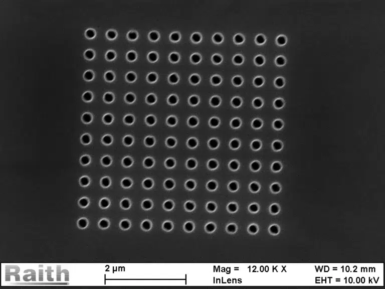
For such a complicated piece of equipment, it is remarkably easy to learn. RAITH’s manuals are descriptive and comprehensive, but also include tutorials that give you step-by-step directions for common tasks. The software is intuitive, but also powerful and flexible (e.g. there are multiple ways to perform the same function). A new user can start writing real patterns after just a few hours of training. An undergraduate summer student recently developed a process to pattern metal on silicon with features down to <20 nm, successfully fabricating the smallest Queen’s University logo in existence (only 67 µm across).
Support from RAITH has been exceptional. From marketing to applications to technical support, RAITH staff have been helpful and great to deal with. Having a dedicated team in North America has been particularly helpful for us.”


“At the University of Queensland, we recently bought two Raith EBL systems: the eLINE Plus, which was commissioned in 2017, and the EBPG, which arrived in 2018. This has revolutionised […]

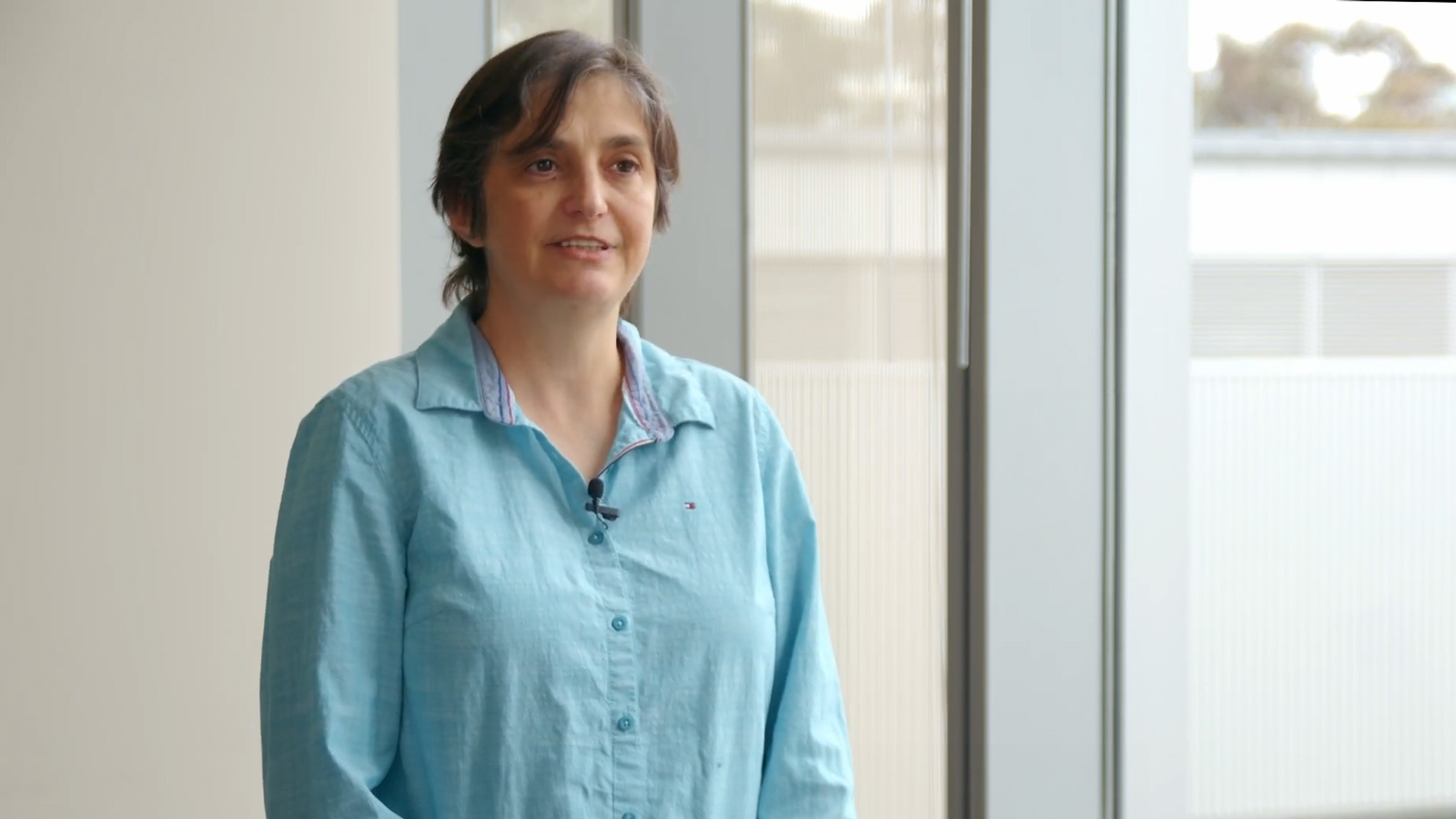
The main user and specialist of the EBPG installed at UCSD is Maribel Montero. She provides insights into her daily work with the system and explains why she is a satisfied RAITH […]