Introduction
The VOYAGER is an EBL system combining stable high performance and ease of use at an attractive price / performance ratio throughout its lifetime, making it a versatile solution for both academic and industrial settings. Its fully automated, ultra-ergonomic design, with smart features and innovative architecture, ensures the shortest time to results. In addition, the inclusion of an environment-tolerant shield guarantees system stability even in less-than-ideal laboratory environments, further enhancing its reliability and usability.
Key features
- Highly ergonomic human-machine interface
- 50 kV thermal field emission column technology
- Fully automated write field calibration
- Automatic focus and stigmator setup
- Automatic switch between high-resolution and high-throughput writing modes
- Flexible directional shape-filling modes
- Stitching-error-free continuous writing modes
- Unique formula-based patterning technology
Benefits
System stability and ease of use even in less ideal laboratory environments
High system stability
The VOYAGER system embodies innovation and stability, offering consistent high performance throughout its lifetime. Its environment-tolerant shield ensures system stability even in less ideal laboratory environments, providing reliability and repeatability of EBL results.
Shortest time to result
The intuitive user interface offered by the RAITH Nanosuite, in conjunction with the new ErgoFlow user interface, including fully automated “push-button-like” exposure capabilities, delivers shortest time to result without time-consuming iterations required for EBL result optimization.
Application specific solutions
VOYAGER offers innovative and unique features that advance the quality and performance of specific devices. Whether in nanophotonic or optoelectronic applications, stitch-error-free continuous writing modes or algorithmic patterning solutions help yield optimum results.


Perfect
Shapes

Smart
Motion

Auto
Run
Software
Digital RAITH is the infrastructure for any nanolithography applications

Designed for automated exposure operations
The proprietary Digital RAITH Nanosuite control software, with its various modules, is the most comprehensive and fully integrated nanolithography software available.
GDSII CAD layout editor
The integrated professional layout design editor/viewer eliminates the need for third-party software, streamlining data import and conversion processes.
Mix and Match capabilities
Whether your application involves contacting nanoscaled features, automatic mark recognition for perfect overlay, multilevel lithography, or combining different lithography techniques, the RAITH Nanosuite delivers adequate functionalities and workflows.
Full exposure job automation & customization
System operators can control all system functionalities and exploit its capabilities from a single software platform, eliminating the need to exchange data between different programs.
Dedicated imaging and metrology functionality
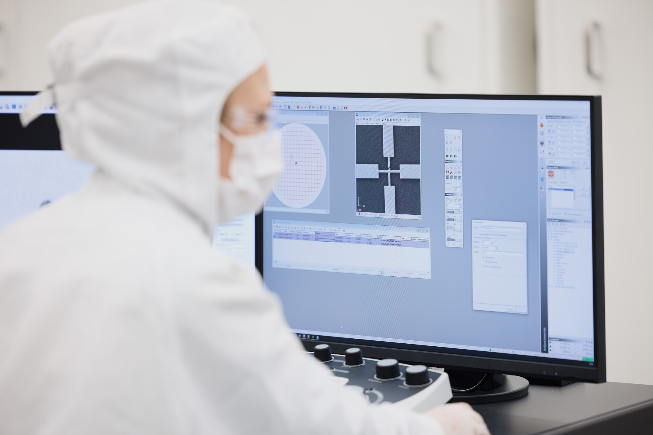
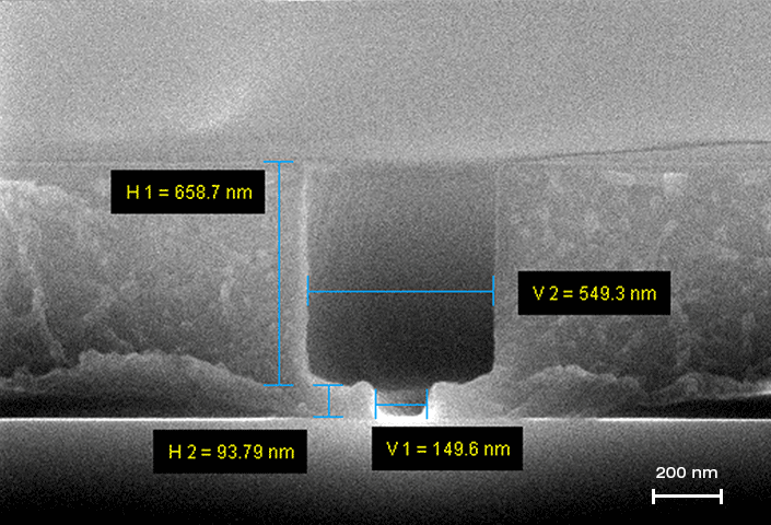
As a lithographer, you want to expose your sample and also verify your design. To ensure that your sample’s structures meet the dimensionality of the original design, the Digital RAITH Nanosuite offers comprehensive imaging and metrology capabilities.
True multi-user environment
RAITH Nanosuite offers more than Windows Explorer – like data administration. User authentication is required for logging in, and different user levels allow access to specific sensitive system parameters. Each user finds the system as they left it and doesn’t interfere with others.
Proximity effect correction
RAITH Nanosuite ensures physics are considered throughout integrated proximity effect corrections. Complex electron interactions in resist and in the sample sometimes require comprehensive optimization of local dose distribution. The integrated proximity effect correction ensures highest pattern fidelity when applied to original GDSII design and can simulate 3D resist profiles.
3D / grayscale lithography
Knowing the resist contrast curve is essential for properly transferring equidistant gray levels into your resist. The RAITH Nanosuite supports resist contrast curve data import and calculates appropriate local dose distribution accordingly.
GDSII-patterning on image
RAITH Nanosuite can acquire an image and directly overlay a GDSII design onto it without the need for time-consuming overlay or mark recognition procedures. This can drastically speed up nanocontacting applications, and deposition or milling jobs.
Continuous and stitch-error-free patterning modes
RAITH is the only company that offers patterning modes based on RAITH proprietary FBMS- and MBMS-technology, where the stage is continuously moving during an exposure and is following a pre-defined path, thus avoiding stitching errors.
Algorithmic patterning
Specific applications require efficient data handling and precise control over beam shot placements. Algorithmixx offers both to efficiently shorten overhead times and increase pattern fidelity.
100 person-years of software programming
Technical data
≤ 8 nm
Guaranteed min. linewidth
≤ +/- 0.2 %
Beam current stability per hour
≤ 40 nm
Minimum grating periodicity
Max. write
field size
field size
Stitching
Overlay
Beam position stability
(without drift correction)
(without drift correction)
Full travel range laser
interferometer stage
interferometer stage
Are you interested in more details and insights?
VOYAGER Product Brochure (.pdf)
Application pattern
Bringing applications to perfection
Solutions
RAITH offers integrated solutions that increase performance and create market opportunities. In any production environment.
Patterning
By eliminating stitching errors, our solution guarantees optimal performance and reliability, driving breakthroughs.
Mix and Match
Seamless blending of laser direct writing, ion beam, and electron beam technologies, unlocking new nanostructuring horizons.
Digital RAITH
Mature software engineering for seamless integration, efficient task support, and user-friendly operation.
It should be no surprise that we are not able to share project details here. Suffice to say that we’re proud of the work we did with some well-known global tech leaders and leading scientific institutions.


