Introduction
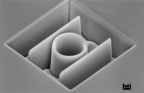
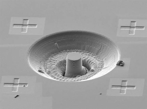
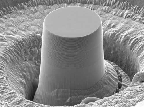
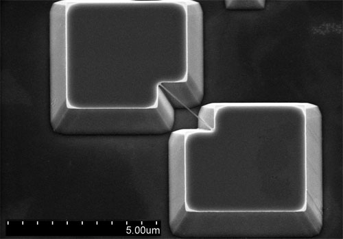
Nanopatterning made simple: ELPHY stands for the easiest and most economical access to professional nanolithography and nanofabrication. It provides all you need to efficiently start to enter the nanolithography world. The upgrade kits, also known as “lithography attachments”, enable virtually any SEM or FIB to be converted into a nanolithography or nanofabrication station in order to unlock and fully exploit its nanopatterning potential – without sacrificing any of its original functionality!
Benefits
Create your own nanolithography system
Highest flexibility and cost-effectiveness
Depending on the SEM or FIB-SEM performance, your specific applications and related requirements for stability or ultimate precision, and finally your budget, there are 3 different ELPHY systems to choose from according to your needs.
Access to the Digital RAITH Nanosuite
No other system can match the RAITH software suite in terms of flexibility, intuitiveness, and ease of use – all embedded in a true multi-user management system. All advanced and fully integrated software modules, well established and also used in higher grade RAITH EBL turnkey systems, can be accessed already with ELPHY.
Much more than EBL functionality only
ELPHY MultiBeam includes all comprehensive multiple technique nanopatterning functionality in a single tool, not limited to Electron Beam Lithography (EBL). It is also suited for Focused Ion Beam Nanofabrication, gas-assisted Focused Electron- or Ion Beam Induced Processes (FEBIP/FIBIP), like etching or deposition, and Helium ion beam patterning.

Software
Electron beam lithography control software for nanopatterning: Nothing compares!
Designed for automated exposure operations
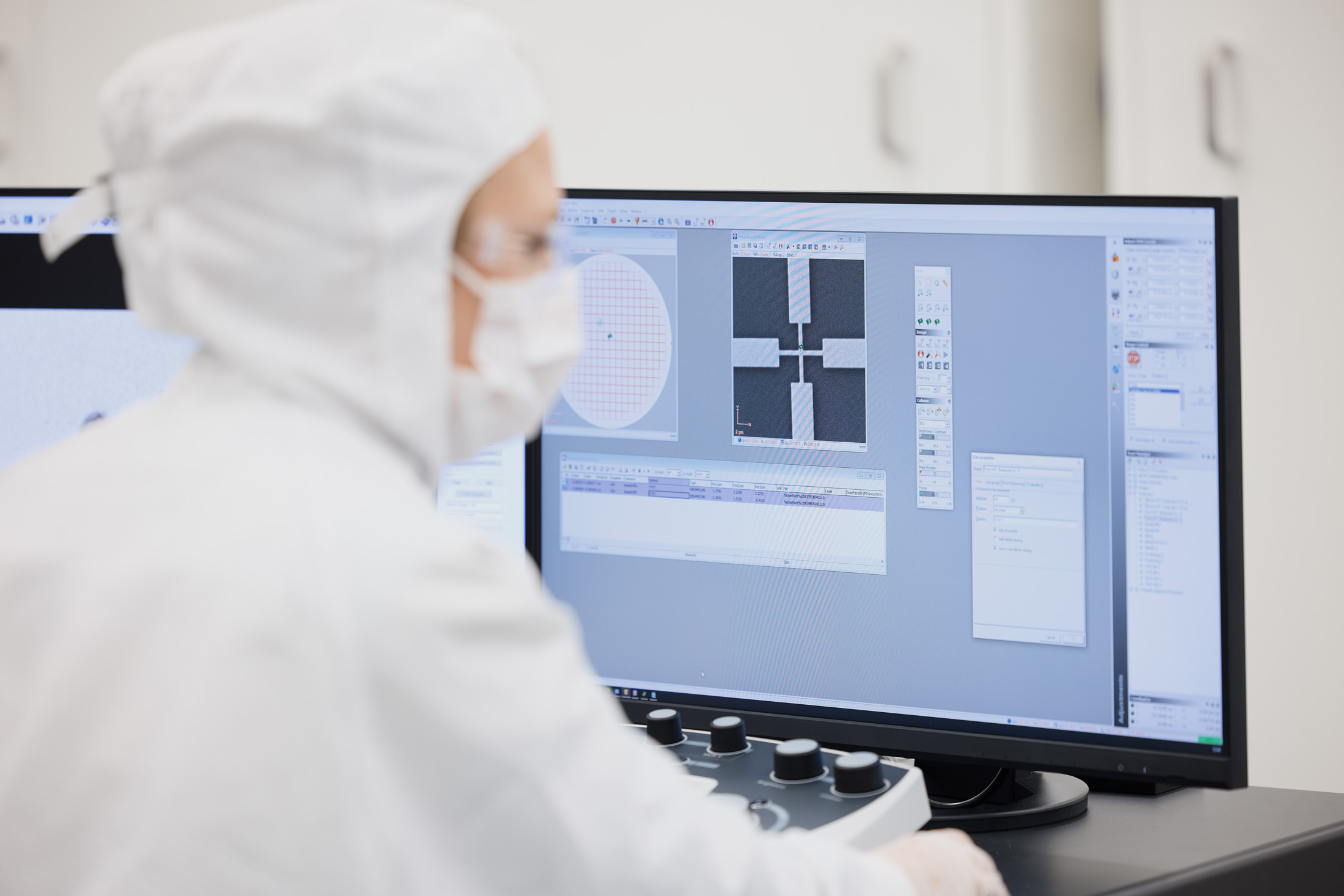
The proprietary Digital RAITH Nanosuite control software, with its various modules, is the most comprehensive and fully integrated nanolithography software available.
GDSII CAD layout editor
The integrated professional layout design editor / viewer eliminates the need for third-party software, streamlining data import and conversion processes.
Mix and Match capabilities
Whether your application involves contacting nanoscaled features, automatic mark recognition for perfect overlay, multilevel lithography, or combining different lithography techniques, the RAITH Nanosuite delivers adequate functionalities and workflows.
Full exposure job automation & customization
System operators can control all system functionalities and exploit its capabilities from a single software platform, eliminating the need to exchange data between different programs.
Dedicated imaging and metrology functionality
As a lithographer, you want to expose your sample and also verify your design. To ensure that your sample’s structures meet the dimensionality of the original design, the Digital RAITH Nanosuite offers comprehensive imaging and metrology capabilities.
True multi-user environment
RAITH Nanosuite offers more than Windows Explorer – like data administration. User authentication is required for logging in, and different user levels allow access to specific sensitive system parameters. Each user finds the system as they left it and doesn’t interfere with others.
Proximity effect correction
RAITH Nanosuite ensures physics are considered throughout integrated proximity effect corrections. Complex electron interactions in resist and in the sample sometimes require comprehensive optimization of local dose distribution. The integrated proximity effect correction ensures highest pattern fidelity when applied to original GDSII design and can simulate 3D resist profiles.
3D / grayscale lithography
Knowing the resist contrast curve is essential for properly transferring equidistant gray levels into your resist. The RAITH Nanosuite supports resist contrast curve data import and calculates appropriate local dose distribution accordingly.
GDSII-patterning on image
RAITH Nanosuite can acquire an image and directly overlay a GDSII design onto it without the need for time-consuming overlay or mark recognition procedures. This can drastically speed up nanocontacting applications, and deposition or milling jobs.
100 person-years of software programming
Technical data
20 MHz
Max. writing frequency
8x16 bit DACs
2 main 16 bit DACs and 2x3
multiplying DACs for calibration
multiplying DACs for calibration
Max. patterning frequency
Min. dwell time increment
Outputs
Thermostabilization
Colored touch screen display
Signal router, end point detection
Are you interested in more details and insights?
ELPHY Product Brochure (.pdf)
Application pattern
Single write field applications across all scientific disciplines
Solutions
RAITH offers integrated solutions that increase performance and create market opportunities. In any production environment.
Digital RAITH
Mature software engineering for seamless integration, efficient task support, and user-friendly operation.
Mix and Match
Seamless blending of laser direct writing, ion beam, and electron beam technologies, unlocking new nanostructuring horizons.
Patterning
By eliminating stitching errors, our solution guarantees optimal performance and reliability, driving breakthroughs.
Our customers are excited with their experiences using our products. They emphasize the precision, versatility, and reliability of our ELPHY system series, highlighting how it has improved their approach to nanotechnology and advanced electronics manufacturing.
