Introduction
CHIPSCANNER delivers the most accurate, homogeneous, large-area, high-resolution mosaics on the market. Square centimeter-large areas of any given substrate can be scanned with nanometer resolution and excellent layer-to-layer accuracy for 3D model, layout, and schematic extraction.
Benefits
SEM imaging taken to new dimensions
High precision
The unique laser interferometer stage, combined with field-of-view correction, minimizes overlap and computing, resulting in superior results. With the absolute position of each pixel known, even over cm², images can be vertically stacked with exceptional precision (3D-stitching), ideal for IC analysis 3D modelling.
Enhanced accuracy
Ensure continuous focus over extended distances and curved surfaces with our optional laser-based height sensing module, enhancing imaging capabilities for diverse applications.
High resolution
Integrate high-resolution electron optics, multiple efficient electron detectors, and ultra-precise laser interferometer stage technology for scanning surfaces up to cm² areas with nanometer resolution. Stable brightness / contrast values are guaranteed by a very stable TFE filament and model-dependent temperature stabilization, minimizing drift for high-quality large-area image mosaics.
High throughput
High-speed detectors, flexible working distances, parallel detector stream handling, and on-the-fly corrected scan generator enable fast, precise, and flexible image acquisition. Fully automated load lock with a travel range of up to 150 mm x 150 mm allows loading multiple samples for continuous scanning over days with stable performance. Automated tilt correction and adjustment eliminate the need for human intervention during runs.


Fast
Scan

Ultra
Positioning
Software
Digital RAITH is the infrastructure for any nanolithography applications

Designed for automated exposure operations
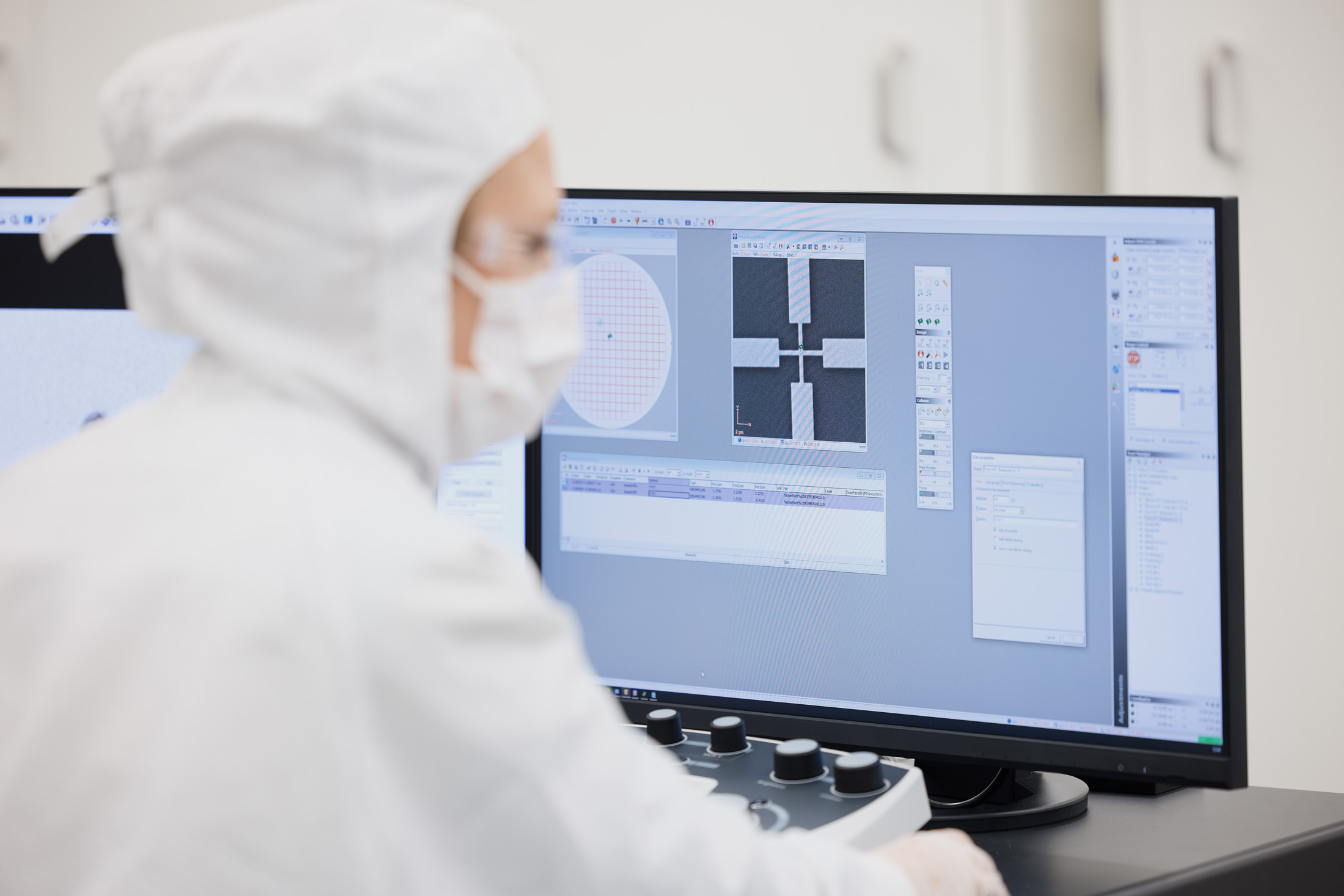
Digital RAITH is the infrastructure for any nanofabrication application, whether for patterning, imaging, or metrology. Powerful software functions optimize scanned mosaic images, converting them into CAD and refining the extracted CAD design for mask layouting.
Sample levelling (automatic on 6-inch systems)
Powerful customizable adjustments and calibrations
Distortion free images
Large area accuracy for 3D stacking
High-speed image scanning with various detectors
Image to CAD conversion
CAD optimization
High-speed mosaic viewer for result analysis
100 person-years of software programming
Technical data
Beam position stability
≤ 200 nm / 8 hrs
Beam current stability
≤ 0.5% / 8 hrs
Image stitching with 100 µm FOV
|mean| + 3σ ≤ 30.0 nm
Stage travel range XY
Load lock type
Maximum wafer size
Environmental shield
Sample tilt & calibration
Are you interested in more details and insights?
CHIPSCANNER Product Brochure (.pdf)
Application pattern
Bringing applications to perfection
Solutions
RAITH offers integrated solutions that increase performance and create market opportunities. In any production environment.
Mix and Match
Seamless blending of laser direct writing, ion beam, and electron beam technologies, unlocking new nanostructuring horizons.


