Introduction
Photonic integrated circuits (PICs) are a versatile technology with a wide range of applications. They are used extensively in telecommunications, data communications, sensing, and biomedical technology. PICs are particularly useful in fiber-optic communication systems because they allow high-speed data transmission over long distances. They are also used in data centers for high-speed interconnects between servers and storage devices. In sensing applications, PICs provide high sensitivity and accuracy, making them ideal for use in gas sensing systems. In biomedical technology, PICs enable non-invasive imaging techniques like optical coherence tomography, which is used for medical diagnosis.
Application
Optical Transceiver
Optical transceivers are crucial components in modern telecommunications. They encode electrical signals into optical signals and convert incoming optical signals back into electrical signals for data transmission and reception over optical fiber networks. Optical transceivers consist of integrated circuits containing various optical and electronic components, including laser diodes, waveguides, modulators, and photodetectors. Facilitating higher levels of integration on photonic integrated circuits in optical transceiver technology leads to higher data rates, longer transmission distances, and improved energy efficiency, driving the evolution of modern networking infrastructure. For instance, incorporating electro-absorption modulators (EAMs) into the receiver architecture eliminates the need for separate modulators and detectors, which leads to compact and more efficient transceiver designs.

Metalens structure using efficient formula based patterningMetalens structure using efficient formula based patterningMetalens structure using efficien

150 nm gate in PMMA (bi-layer)

Freestanding multi-terminal graphene device M. Kühne, MPI Stuttgart, Germany
Application
Gratings in photonic integrated circuits
Gratings are fundamental components of photonic integrated circuits, serving various functions in manipulating light. They are used as wavelength-selective filters, grating couplers, mode converters, and wavelength multiplexers/demultiplexers.Electron beam lithography allows for precise control over their dimensions and properties, including control of the grating pitch with sub-nanometer accuracy. Gratings are essential optical components for various applications in optical communication, sensing, and signal processing within photonic integrated circuits.

Metalens structure using efficient formula based patterningMetalens structure using efficient formula based patterningMetalens structure using efficien

150 nm gate in PMMA (bi-layer)

Freestanding multi-terminal graphene device M. Kühne, MPI Stuttgart, Germany
Application
Ring resonator
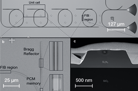
A ring resonator is a closed-loop waveguide, typically made of a high-refractive-index material such as silicon nitride. Light is coupled into the ring resonator, where it circulates around the loop multiple times. This results in constructive interference between the incoming and circulating light waves at specific resonance wavelengths, enhancing the transmission of light at those wavelengths. This creates sharp resonant peaks in the transmission spectrum. The performance and resonance wavelength of the ring resonator are sensitive to variations in its dimensions, which means fabrication requires precise patterning techniques.
Post-fabrication tuning of the optical path length using ion implantation can control the resonance wavelength with an accuracy below 10 pm. Ring resonators are utilized in various photonic applications such as filters, modulators, sensors, and wavelength converters due to their ability to selectively filter or enhance specific wavelengths of light based on their resonant properties. They offer compact size, high-Q (quality factor), and compatibility with standard semiconductor fabrication processes, making them essential building blocks for miniaturized photonic devices and integrated circuits.
Post-fabrication tuning of the optical path length using ion implantation can control the resonance wavelength with an accuracy below 10 pm. Ring resonators are utilized in various photonic applications such as filters, modulators, sensors, and wavelength converters due to their ability to selectively filter or enhance specific wavelengths of light based on their resonant properties. They offer compact size, high-Q (quality factor), and compatibility with standard semiconductor fabrication processes, making them essential building blocks for miniaturized photonic devices and integrated circuits.

Wavelength addressable photonic memory, Akhil Varri, University of Münster, Germany

150 nm gate in PMMA (bi-layer)

Freestanding multi-terminal graphene device M. Kühne, MPI Stuttgart, Germany
Are you interested in more details and insights?
Application
TFNL modulator
Electro-optical modulators (EOMs) are critical components in optical telecommunications systems, playing a vital role in encoding information onto optical signals for transmission over fiber optic networks. These modulators utilize the electro-optic effect in materials like lithium niobate, which causes changes in the refractive index of certain materials when an electric field is applied. The fabrication of thin-film lithium niobate on insulator (LNOI) substrates allows for the integration of lithium niobate into compact photonic integrated circuits, enabling the miniaturization of EOMs and other optical components. Recent developments in thin-film lithium niobate (TFLN) modulators - primarily based on fabrication with electron beam lithography - have garnered significant attention due to their potential for high-performance and compact devices. TFLN modulators offer advantages such as high modulation speed, low power consumption, and compatibility with existing photonic integration platforms. Ongoing research aims to enhance further the performance and integration capabilities of TFLN modulators for next-generation photonic technologies.

Metalens structure using efficient formula based patterningMetalens structure using efficient formula based patterningMetalens structure using efficien

150 nm gate in PMMA (bi-layer)

Freestanding multi-terminal graphene device M. Kühne, MPI Stuttgart, Germany
Are you interested in more details and insights?
Application
Photonic crystals
Photonic crystals are composed of periodic arrays of dielectric materials with alternating refractive indices that create band gaps, which hinder the propagation of specific wavelengths of light. These bandgaps allow for the localization and manipulation of light within the photonic crystal structure, enabling various functions in photonic integrated circuits such as light confinement, filtering, and dispersion control. Fabricating circular holes with excellent uniformity and placement is crucial for their performance. Advanced patterning techniques for photonic crystals include efficient pattern generation of circular shapes and proximity effect correction that compensates for dose variations caused by backward electron scattering.

Photonic crystal nanobeam laser structure, Aura Higuera Rodriguez, Eindhoven University of Technology, Netherlands

150 nm gate in PMMA (bi-layer)

Freestanding multi-terminal graphene device M. Kühne, MPI Stuttgart, Germany
Are you interested in more details and insights?