Laser

Introduction

Semiconductor lasers play a crucial role in modern optical telecommunication systems. They enable high-speed data transmission over long distances. To meet the growing demand for faster data rates, these lasers need to be modulated at high frequencies. Additionally, for wavelength division multiplexing, the emission wavelength must be precisely and stably controlled using integrated DFB or DBR gratings.
Application

DFB and DBR laser

DFB (Distributed Feedback) and DBR (distributed Bragg reflector) lasers are semiconductor lasers using a grating structure to provide optical feedback, ensuring single-mode operation and precise wavelength control by grating pitch definition with sub-nm accuracy. Different types of gratings are utilized to tailor the optical properties and improve performance. Phase-shifted gratings incorporate intentional discontinuities to modify the interference pattern and enhance laser characteristics like linewidth and side mode suppression ratio. Superstructure gratings introduce additional periodicities within the grating pattern, enabling more complex emission spectra and improved performance in specific applications. Chirped gratings feature a spatial variation in the grating period, broadening the laser’s emission spectrum for applications such as optical coherence tomography and spectroscopy. Advanced electron beam lithography techniques are crucial for precise grating structure control. Ultimately, the fabrication significantly influences the behavior and capabilities of DFB lasers, catering to diverse application requirements in telecommunications, sensing, and spectroscopy.
Image of a 2mm long DFB laser
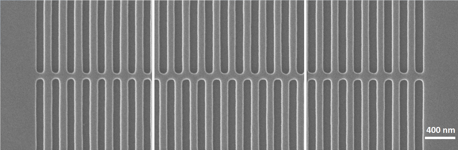
Start-, middle-, and end-section of two 2 mm long gratings. With 200.000 (upper) and 200.020 nm (lower grating) they almost look the same. The difference of 20 pm becomes visible in the number of periods (10000 in the upper, 9999 in the lower grating).
150 nm gate in PMMA (bi-layer)
Freestanding multi-terminal graphene device M. Kühne, MPI Stuttgart, Germany
Are you interested in more details and insights?
Application

VCSEL

Vertical-cavity surface-emitting lasers (VCSELs) are semiconductor-based light sources that emit light perpendicular to the surface of the chip, unlike traditional edge-emitting lasers. They are compact and efficient, widely used in optical communication, sensing, and consumer electronics. VCSELs consist of a semiconductor chip with multiple layers, including an active region where light is generated. VCSELs can be fabricated in arrays, allowing for parallel data transmission in optical communication networks. The vertical cavity confines light within the structure, enabling efficient emission. Confinement by the top layer can be designed for single-mode emission or coupling several VCSELs for coherent emission. Fabricating the required nanostructures involves using photonic crystal cavity arrays that require advanced patterning techniques, like those used for photonic crystals.
Metalens structure using efficient formula based patterningMetalens structure using efficient formula based patterningMetalens structure using efficien
150 nm gate in PMMA (bi-layer)
Freestanding multi-terminal graphene device M. Kühne, MPI Stuttgart, Germany
Are you interested in more details and insights?
Application

Microlens array

Micro-lens arrays are used for coupling light into optical fibers, aligning optical components, and shaping light beams in telecommunication systems. They help improve signal transmission efficiency and reduce losses in optical networks. Grayscale laser beam lithography allows direct pattering of 3D-shaped lenses, usually for fabrication of imprint masters or prototyping. Key elements are flexible design software, including contrast curve corrections, pattering with high dynamic range for best grayscale performance, and cutting-edge thick resist processing.
Image of a micro lens array
Micro lens array made on a Si substrate with the direct laser writer PICOMASTER. Individual lens width is 20 µm at the bottom. Height of each lens 10 µm. Due to the perfect grayscale performance of the tool a smooth structure profile was achieved with high repeatability
150 nm gate in PMMA (bi-layer)
Freestanding multi-terminal graphene device M. Kühne, MPI Stuttgart, Germany

Discoveries and innovations

Insights

To find out which configuration best suits your needs, get in touch with us.
I want to contact a RAITH-Expert
Headline
This is a basic text element.
Headline
This is a basic text element.